TSMC says its newest process tech doesn't need ASML's High-NA EUV chipmaking tools that have been championed by Intel, but the foundry is exploring the tech for future use.
According to Reuters, Zhang told attendees of the event that the A16 process technology will not need the next-generation EUV lithography tools. This implies means that TSMC has found ways to cost-efficiently use EUV double patterning and pattern shaping to increase the achievable critical dimension of a modern Low-NA litho system beyond 13nm. In contrast, Intel plans to insert High-NA EUV tools with its 14A manufacturing technology after it learns how to efficiently use them with its 18A production node.
TSMC is not standing still, though. The company is exploring High-NA EUV lithography for its future process technologies. The A14 node will follow A16, and as TSMC noted in its 2023 Annual Report, A14 development is well underway.
"TSMC started development and made good progress on 14 Angstrom (A14) technology, which aims to further improve speed, power, density and cost," the company's Annual Report reads. "Looking ahead to A14 and beyond, TSMC R&D will continue to explore next generation EUV (extreme ultraviolet) lithography scanners, conduct research on mask pellicles and blanks to support leading-edge technology and extend Moore's Law."
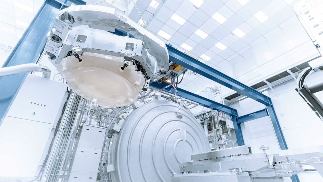
Using High-NA EUV lithography systems greatly increases fab costs as each tool costs $385 million or more depending on the configuration. Chipmakers tend to re-use as many tools as possible, so TSMC may not be inclined to use High-NA EUV before it runs out of ways to introduce improvements to its production capabilities using Low-NA EUV tools. For example, last year, the company improved the critical dimension and pattern fidelity as well as lowered defect density by modifying photoresist and blank materials as well as optimizing mask process recipes. It also uses deep learning for inspection and discovering defects.
"In 2023, to achieve the wafer yield and productivity for lithography requirements at 2nm node, the R&D team improved the critical dimension, pattern fidelity, overlay stability, exposure durability, and defect mitigation of curvilinear patterns by EUV photoresist and blank material modification, multi-beam writer resolution enhancement, mask process recipe optimization, and advanced deep learning inspection," TSMC said in the report. "Future improvements will focus on developing new blank materials and new mask process technology at the A14 node and beyond."
TSMC's announcement of its A16 process technology (1.6nm-class) with Super Power Rail backside power delivery came as a surprise at the company's North America Technology Symposium 2024. Kevin Zhang, Vice President of Business Development at TSMC, said that the world's largest contract chipmaker had to speed up development of the production node due to rising demand from the AI sector, reports Reuters.