
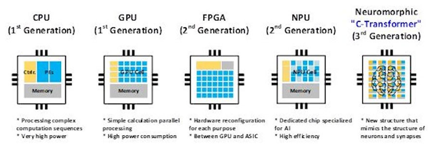
A team of scientists from the Korea Advanced Institute of Science and Technology (KAIST) detailed their 'Complementary-Transformer' AI chip during the recent 2024 International Solid-State Circuits Conference (ISSCC). The new C-Transformer chip is claimed to be the world's first ultra-low power AI accelerator chip capable of large language model (LLM) processing.
In a press release, the researchers power-shame Nvidia, claiming that the C-Transformer uses 625 times less power and is 41x smaller than the green team's A100 Tensor Core GPU. It also reveals that the Samsung fabbed chip's achievements largely stem from refined neuromorphic computing technology.
Though we are told that the KAIST C-Transformer chip can do the same LLM processing tasks as one of Nvidia's beefy A100 GPUs, none of the press nor conference materials we have provided any direct comparative performance metrics. That's a significant statistic, conspicuous by its absence, and the cynical would probably surmise that a performance comparison doesn't do the C-Transformer any favors.
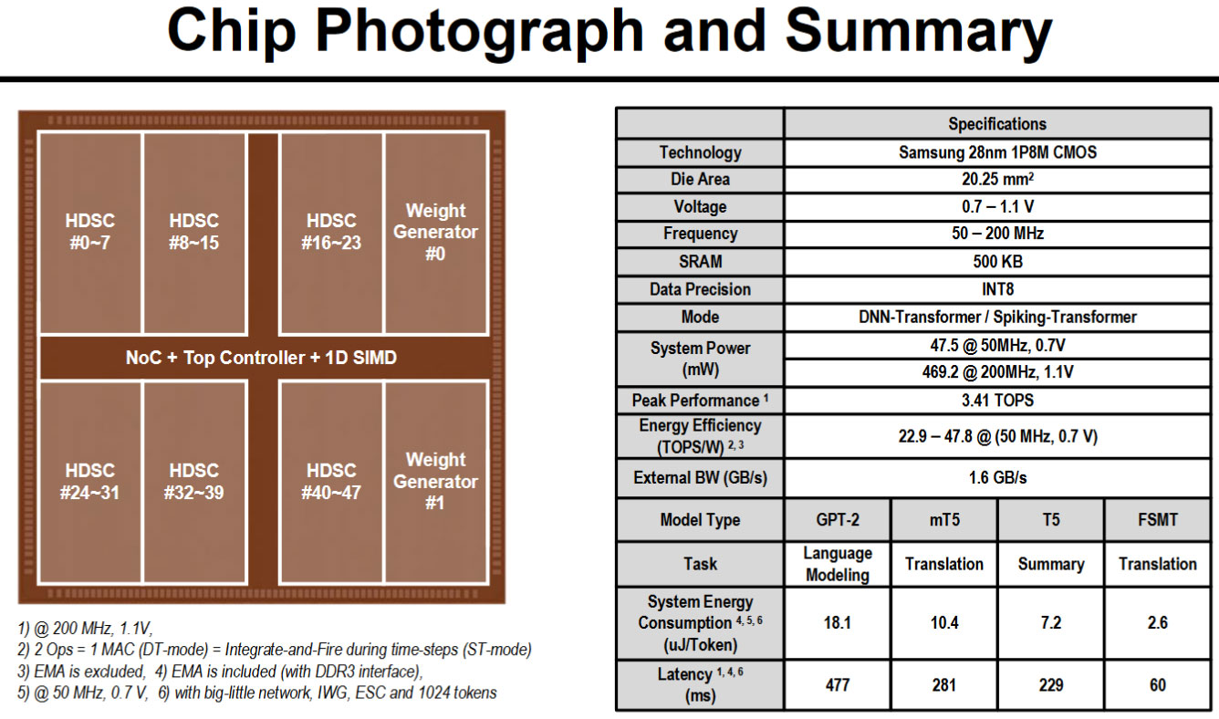
The above gallery has a 'chip photograph' and a summary of the processor's specs. You can see that the C-Transformer is currently fabbed on Samsung's 28nm process and has a die area of 20.25mm2. It runs at a maximum frequency of 200 MHz, consuming under 500mW. At best, it can achieve 3.41 TOPS. At face value, that's 183x slower than the claimed 624 TOPS of the Nvidia A100 PCIe card (but the KAIST chip is claimed to use 625x less power). However, we'd prefer some kind of benchmark performance comparison rather than look at each platform's claimed TOPS.
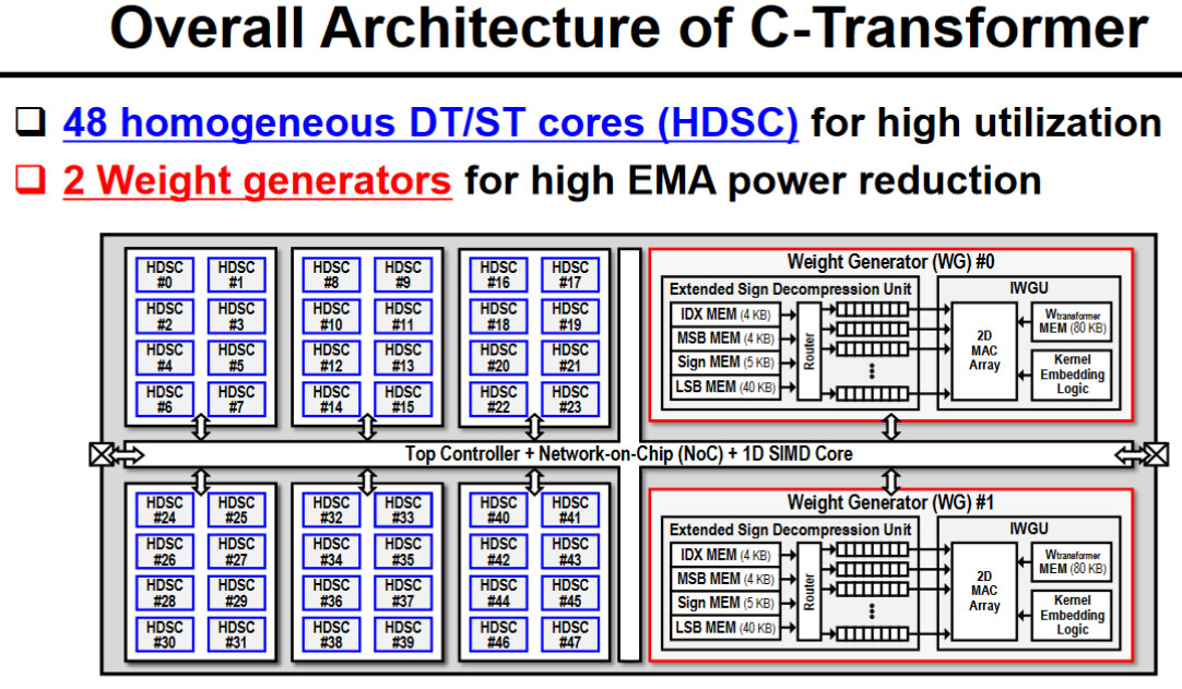
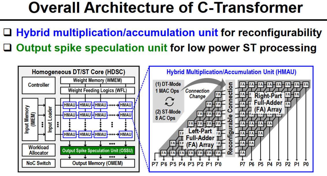
The architecture of the C-Transformer chip is interesting to look at and is characterized by three main functional feature blocks. Firstly, there is a Homogeneous DNN-Transformer / Spiking-transformer Core (HDSC) with a Hybrid Multiplication-Accumulation Unit (HMAU) to efficiently process the dynamically changing distribution energy. Secondly, we have an Output Spike Speculation Unit (OSSU) to reduce the latency and computations of spike domain processing. Thirdly, the researchers implemented an Implicit Weight Generation Unit (IWGU) with Extended Sign Compression (ESC) to reduce External Memory Access (EMA) energy consumption.
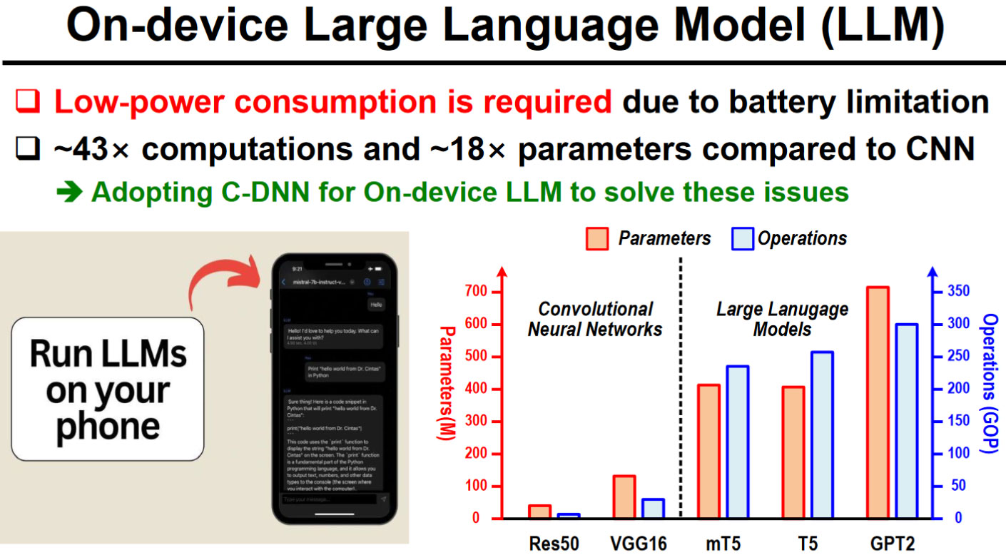
It is explained that the C-Transformer chip doesn't just add some off-the-shelf neuromorphic processing as its 'special sauce' to compress the large parameters of LLMs. Previously, neuromorphic computing technology wasn't accurate enough for use with LLMs, says the KAIST press release. However, the research team says it "succeeded in improving the accuracy of the technology to match that of [deep neural networks] DNNs."
Though there are uncertainties about the performance of this first C-Transformer chip due to no direct comparisons with industry-standard AI accelerators, it is hard to dispute claims that it will be an attractive option for mobile computing. It is also encouraging that the researchers have got this far with a Samsung test chip and extensive GPT-2 testing.