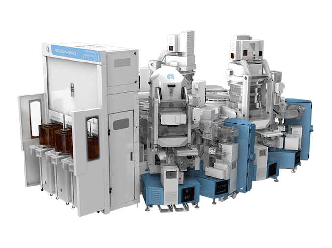
Although the pace of Moore's Law has undeniably slackened in the last decade, transistor density is still increasing with every new process technology. But there is a challenge with feeding power to smaller transistors, as with the smaller transistors comes thinner power wires within the chip, which increases their resistance and may cause yield loss. Looking to combat that effect, this week Applied Materials introduced its new Applied Endura Copper Barrier Seed IMS with Volta Ruthenium Copper Vapor Deposition (CVD) tool, which enables chipmakers to keep using copper for wiring with 2 nm-class and more advanced process technologies.
Today's advanced logic processors have about 20 layers of metal, with thin signal wires and thicker power wires. Scaling down wiring with shrinking transistors presents numerous challenges. Thinner wires have higher electrical resistance, while closer wires heighten capacitance and electrical crosstalk. The combination of the two can lead to increased power consumption while also limiting performance scaling, which is particularly problematic for datacenter grade processors that are looking to have it all. Moving power rails to a wafer's back-side is expected to enhance performance and efficiency by reducing wiring complexity and freeing up space for more transistors.
But backside power delivery network (BSPDN) does not solve the problem with thin wires in general. As lithographic scaling progresses, both transistor features and wiring trenches become smaller. This reduction means that barriers and liners take up more space in these trenches, leaving insufficient room to deposit copper without creating voids, which raises resistance and can lower yields. Additionally, the closer proximity of wires thins the low-k dielectrics, making them more vulnerable to damage during the etching process. This damage increases capacitance and weakens the chips, making them unsuitable for 3D stacking. Consequently, as the industry advances, copper wiring faces significant physical scaling challenges. But Applied Materials has a solution.
Adopting Binary RuCo Liners
Contemporary manufacturing technologies use reflow to fill interconnects with copper, where anneals help the copper flow from the wafer surface into wiring trenches and vias. This process depends on the liners on which the copper flows. Normally, a CVD cobalt film was used for liners, but this film is too thick for 3nm-class nodes (which would affect resistance and yield).
Applied Materials proposes using a ruthenium cobalt (RuCo) binary liner with a thickness under 20A (2nm, 20 angstroms), which would provide better surface properties for copper reflow. This would ultimately allow for 33% more space for void-free conductive copper to be reflowed, reducing the overall resistance by 25%. While usage of the new liner requires new tooling, it can enable better interconnects that mean higher performance, lower power consumption and higher yields.


Applied Materials says that so far its new Endura Copper Barrier Seed IMS with Volta Ruthenium CVD tool has been adopted by all leading logic makers, including TSMC and Samsung Foundry for their 3nm-class nodes and beyond.
"The semiconductor industry must deliver dramatic improvements in energy-efficient performance to enable sustainable growth in AI computing," said Dr. Y.J. Mii, Executive Vice President and Co-Chief Operating Officer at TSMC. "New materials that reduce interconnect resistance will play an important role in the semiconductor industry, alongside other innovations to improve overall system performance and power."
New Low-K Dielectric
But thin and efficient liner is not the only thing crucial for wiring at 3nm production nodes and beyond. Trenches for wiring are filed not only with a Co/RuCo liner and a Ta/N barrier, but with low dielectric constant (Low-K) film to minimize electrical charge buildup, reduce power consumption, and lower signal interference. Applied Materials has offered its Black Diamond Low-K film since the early 2000s.
But new production nodes require better dielectrics, so this week the company introduced an upgraded version of Black Diamond material and a plasma-enhanced chemical vapor deposition (PEVCD) tool to apply it, the Producer Black Diamond PECVD series. This new material allows for scaling down to 2nm and beyond by further reducing the dielectric constant while also increasing the mechanical strength of the chips, which is good for 3D stacking both for logic and memory. The new Black Diamond is being rapidly adopted by major logic and DRAM chipmakers, Applied says.
"The AI era needs more energy-efficient computing, and chip wiring and stacking are critical to performance and power consumption," said Dr. Prabu Raja, President of the Semiconductor Products Group at Applied Materials. "Applied's newest integrated materials solution enables the industry to scale low-resistance copper wiring to the emerging angstrom nodes, while our latest low-k dielectric material simultaneously reduces capacitance and strengthens chips to take 3D stacking to new heights."