AMD recently held its Zen 5 Tech Day, unveiling the details of its soon-to-be-released Ryzen 9000 'Granite Ridge' and Ryzen AI 300 'Strix Point' processors to the world. There was plenty of information, but the company followed up this week with even more deep-dive details on its Zen 5 microarchitecture and SoC layout.
AMD revealed that its Zen 5c 'compact' cores are roughly 25% smaller than the standard full-fat Zen 5 cores and that the two core types have varying amounts of cache on the same die — a first for an AMD design. The company also announced many other interesting technical details, which we'll cover below.
The SoCs and Zen 5c's ~25% reduction in die area
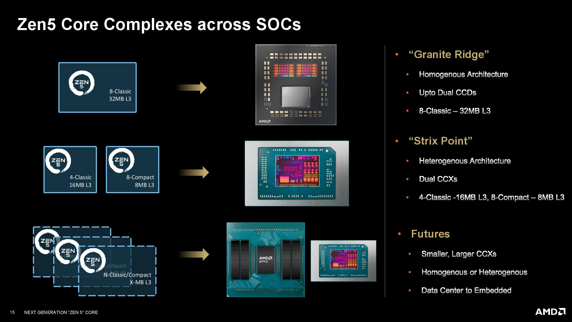
AMD developed the Zen 5 architecture and then customized it for a more compact implementation for its Zen 5c cores. This single architecture, deployed in two customizable core types, will be used for its desktop, mobile, and server processors and span both the 4nm and 3nm process nodes.
AMD's approach to its 'compact' Zen 5c cores is inherently different than Intel's approach with its e-cores. Like Intel's E-cores, AMD's Zen 5c cores are designed to consume less space on a processor die than the 'standard' performance cores while delivering enough performance for less demanding tasks, thus saving power and delivering more compute horsepower per square millimeter than was previously possible (deep dive here). But the similarities end there. Unlike Intel, AMD employs the same microarchitecture and supports the same features with its smaller cores.
AMD's full-fat Zen 5 and compact Zen 5c cores can be used in multiple segments in either heterogeneous designs with both core types on the same die (like Strix Point) or homogeneous designs that only use one core type (like the Granite Ridge desktop chips with only full-sized cores, or the previous-gen EPYC Bergamo server chips with only smaller compact cores).
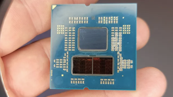
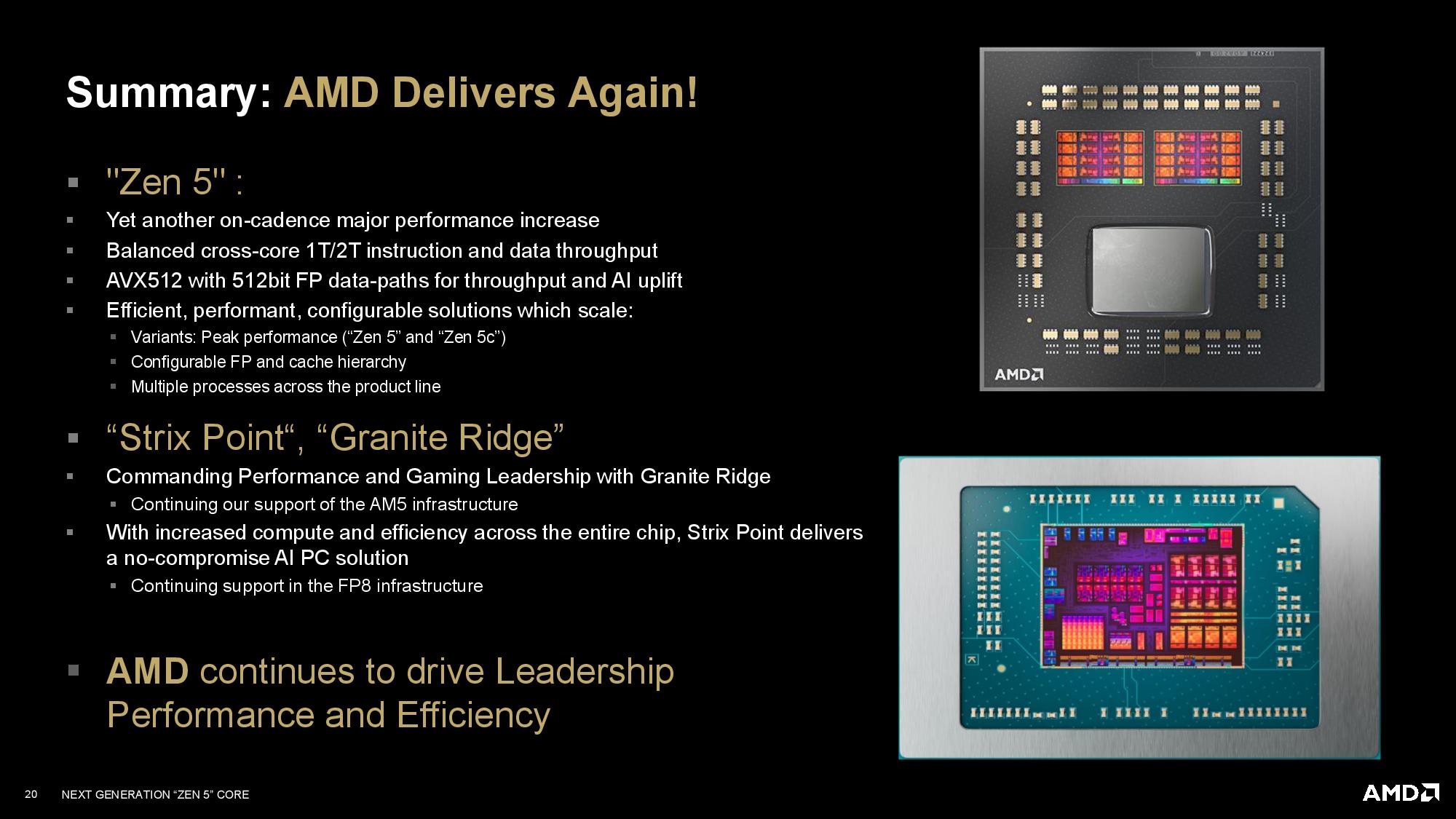
The Ryzen 9000 Granite Ridge processors are exactly as expected — a single CCD (Core Chiplet Die) contains eight full Zen 5 cores paired with 32MB of L3 cache. CPUs will come with either one or two CCDs, paired with an IOD (Input Output Die) that handles many of the other functions present in modern SoCs.
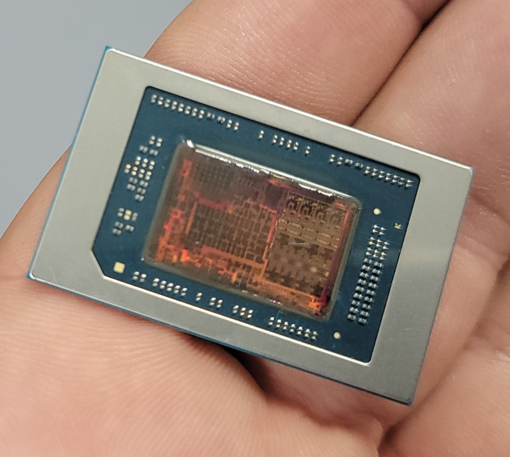
The Strix Point SOC is completely unique. The compact cores are designed for scale-out performance while providing a more optimal power-to-performance ratio. Part of the difference stems from AMD using different cache capacities for this core type.
The die has two CCXs (Core Complexes — core clusters on the same die), much like we saw in older AMD Zen 2 chips. Both core types have their own private L1 and L2 caches, but the 24MB of L3 cache is split into a 16MB slice for the standard cores and an 8MB slice for the Zen 5c compact cores.
AMD's Zen 5c cores mark the first time it has had two core types with different cache capacities on the same die — the four full-sized performance cores have 4MB of L3 apiece to satisfy low-latency and bursty workloads. In contrast, the eight compact cores have a mere 1MB of L3 apiece for low-utilization high-residency workloads.
The reduced L3 cache capacity saves not only area for the compact cores but also drastically reduces power consumption—the chip uses far less power-hungry cache per compact core. Given that AMD would like to run the entire machine on compact cores as much as possible while power-gating the performance cores and their large L3 caches, this has tremendous potential for boosting battery life — provided the scheduling mechanisms work as intended.
The move to an asymmetrical cache design presents new scheduling and management issues for AMD. These two L3 caches have to communicate with each other over the data fabric, much like the CCX-to-CCX cache coherency mechanism found with AMD’s older Zen 2 architecture. This introduces higher latency for cache-to-cache transfers, which AMD says is “not any more than you would have to go to memory for.”
As such, AMD uses Windows scheduler mechanisms to attempt to constrain workloads to either the Zen 5 or 5c cores to reduce the occurrence of high latency transfers, with background workloads typically being assigned to the 5c cores.
Unlike Intel, which prioritizes scheduling work into its E-cores first before it sends it to other cores if the smaller cores aren't fast enough, AMD has no preference for where workloads land first. Instead, AMD allows the operating system to choose the core type to target based on priority and QoS mechanisms, thus ensuring the best possible user experience based on the given workload. AMD has its own thread scheduling mechanisms and provides the OS with tables that enumerate performance and power characteristics for each core, along with providing weights for various operations, thus allowing the OS to make scheduling decisions.
We can also see a breakdown of the EPYC SoC in the slide, with AMD being coy about its next-gen Zen 5 EPYC CPUs by simply listing 'N-Classic/Compact" cores per CCD to keep the lid on core counts for the CCDs — though if tradition holds, this would be the same number of cores per CCD as the desktop parts. We see the same with the "X-MB L3" listing. The "futures" bullet point lists both homogenous and heterogenous types of chips next to the EPYC CCDs, which some could take as implying AMD could have some Zen 5 EPYC chips with mixed core types — that would be a first. However, do note that the bullet point list is an empirical list of features rather than being associated solely with the EPYC CCDs listed next to it.
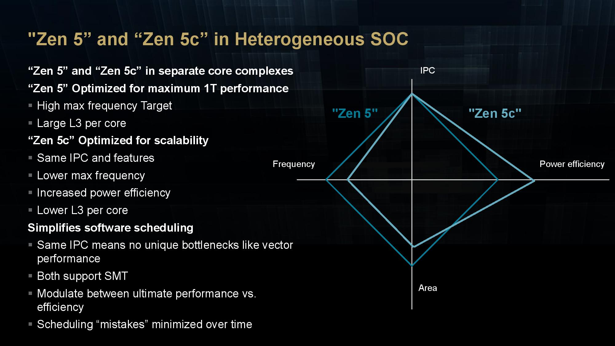
AMD also expanded on its rationale and goals for the Zen 5c compact cores. Unlike Intel's approach, both Zen 5 core types support SMT and the same instruction set (ISA), avoiding the scheduling concerns that Intel faces with its dissimilar core types — Intel's core types don't support the same ISA.
AMD's approach also differs from Intel's because it prioritizes keeping the performance of the Zen 5c cores as close to the standard cores as possible during multi-core workloads. This prevents situations where the larger cores are waiting on smaller cores to complete workloads, which is important for situations like multi-core workloads with thread dependencies. This sidesteps what Mike Clark, Zen's lead architect, calls a 'scheduling cliff,' wherein a large difference in performance will occur if a workload is scheduled into a Zen 5c core, thus negatively impacting the user experience.
Ultimately, the goal is to provide the smallest delta possible between the two core types. So, rather than set the Zen 5c design target predicted by a certain die area requirement, AMD instead targeted a certain voltage/frequency (V/F) curve for the smaller cores.
As with all processors, Zen 5's clock rate will drop as you load more cores due to power and thermal limitations. That means when four performance cores are active, the processor will have a lower clock speed than it does with one active core. AMD used loaded frequency as a guide to decide where to define its V/F curve target for the compact cores, thus keeping the speed delta between the two core types tenable.
Lowering Zen 5c's frequency target allowed the company to break the design down into fewer, bigger blocks that are placed closer together, which confers power reduction benefits. AMD removed the high-speed repeater and buffer circuitry that was no longer needed in 5c cores to hit the maximum frequencies supported by the standard cores. Combined with lower L3 cache capacity per core, Zen 5c's die area was reduced tremendously compared to the standard cores. (You can read more about this in our interview with Clark here.)
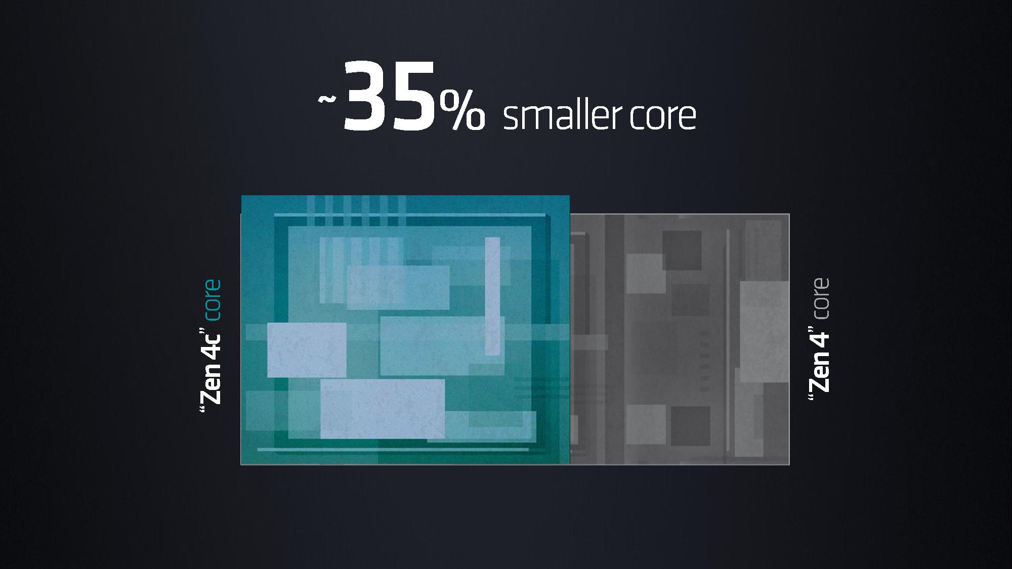
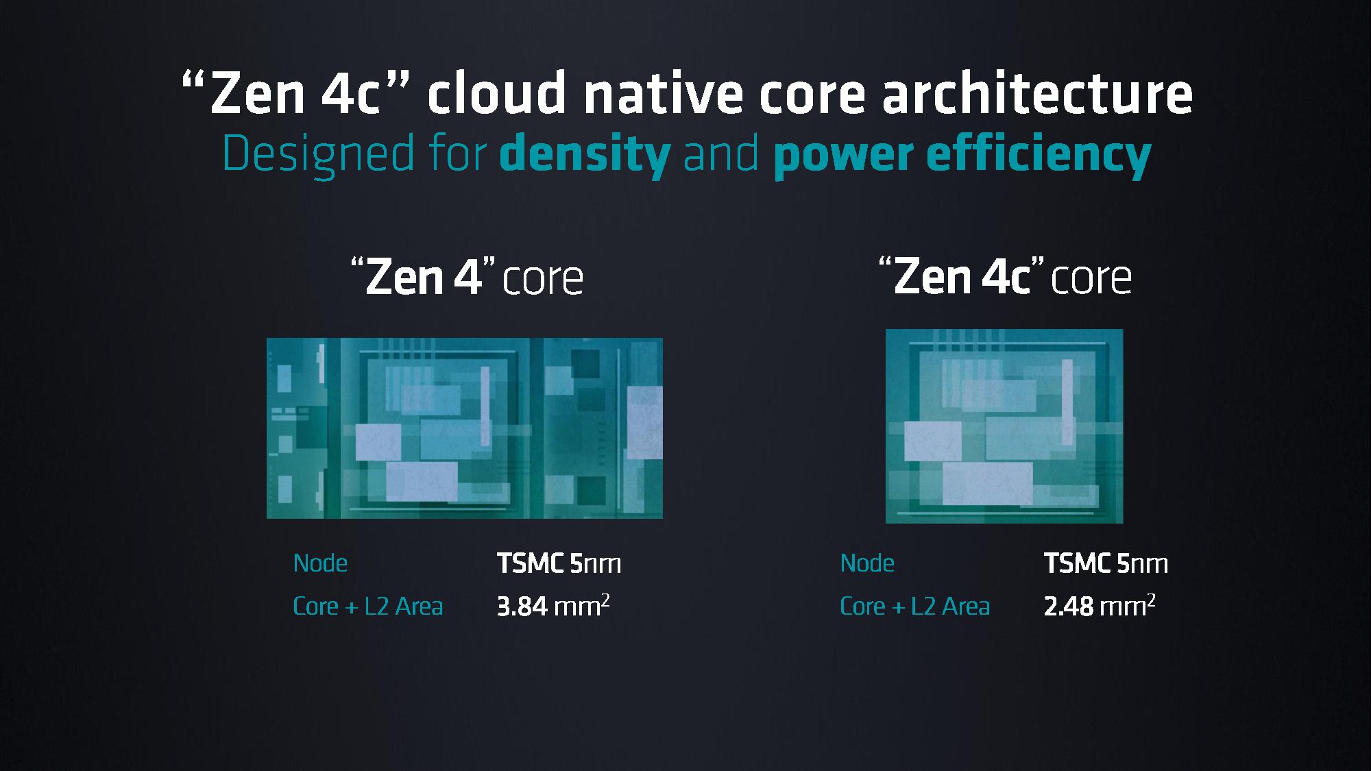
In the end, AMD reduced the area for the Zen 5c cores by around 25% compared to the standard Zen 5 cores (Clark notes this is a ballpark figure). This is less than the 35% reduction we saw with the Zen 4c cores used in the EPYC Bergamo processors (slide above for reference).
Clark said the Zen 5 core could be compacted even further for compact-core-only (homogenous) designs with different performance targets (for reference, Bergamo only has compact cores), but this design meets the targets for this specific heterogenous design. So, it's possible we'll see even denser Zen 5c core designs emerge with other products.
Make no mistake, a 25% reduction in the core area for Zen 5c is impressive, especially if AMD has managed to keep the performance deltas between cores low. However, only testing will tell. We also can't seem to find the clocks for the Zen 5c cores listed on AMD's site, but we're following up for more detail.
AMD Strix Point SoC
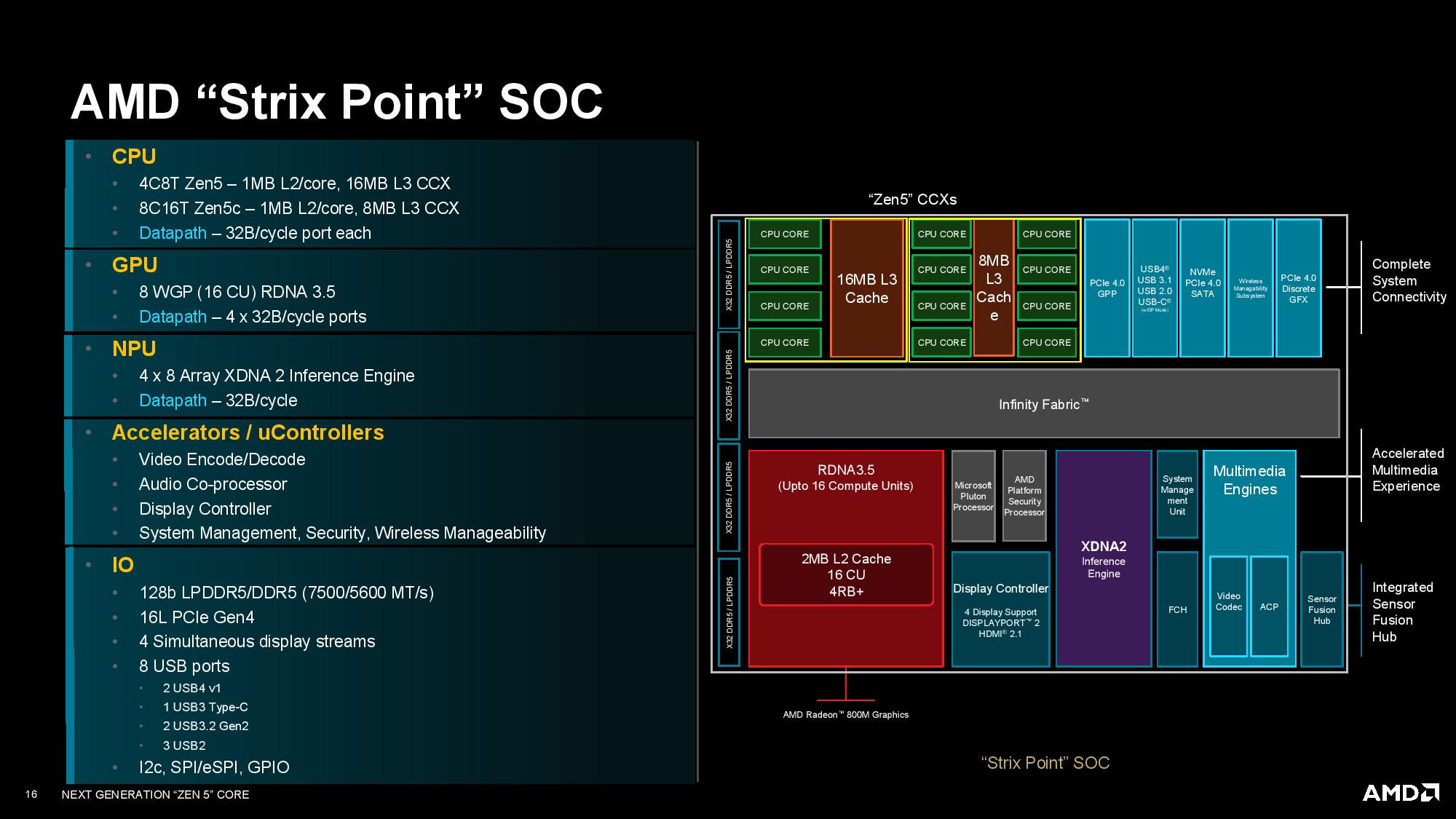
AMD provided the above breakdown of the Strix Point SoC that gives additional details. The most interesting tidbits are the various datapath widths between the different compute units. These datapaths communicate with memory via the Infinity Fabric.
Both Zen 5 and Zen 5c core clusters have their own 32B/cycle port, which means L3 cache-to-cache transfers between the CCXs will have limitations. Meanwhile, the bandwidth-hungry GPU has quad 32B/cycle ports. The XDNA neural processing unit (NPU) also has its own single 32B/cycle interface to the data fabric. We also see the standard complement of fixed-function accelerator blocks, such as video encode/decode and the like. Strix supports LPDDR5-7500 and DDR5-5600 memory.
Notably, AMD cut back on the PCIe lane allocation. As is customary with its mobile parts, AMD steps back to a previous-gen PCIe interface — in this case, PCIe 4.0 — to save power. However, AMD has also dropped from 20 lanes of connectivity to 16, saying this decision was made because the company determined the extra four lanes were almost always used for secondary storage. However, AMD says that use-case isn't common in this segment (low attach rate). As such, AMD determined that reducing the number of lanes was an acceptable trade-off that yielded a pin count reduction that helped save die and substrate area (reduced connections to the die and system board) while further reducing power.
AMD Granite Ridge SoC
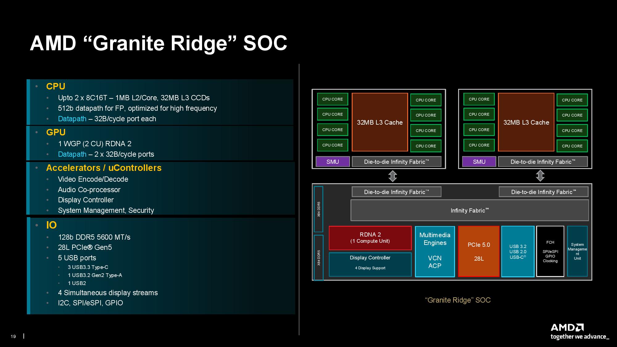
The Granite Ridge SoC in the Ryzen 9000 desktop chips has fewer surprises, with the layout being similar to the previous-gen chips. In fact, the SoC uses the same IOD as the Zen 4 Ryzen 7000 chips. That means CPUs have the same support for DDR5-5600 memory, 28 lanes of PCIe 5.0, five USB ports, and four display streams from the integrated RDNA 2 graphics engine.
Using the same IOD follows AMD's standard policy of smart reuse where possible. The RDNA 2 engine is sufficient for AMD's purposes — it really is just meant to light up a display and not much more. It also allows AMD to keep the same package size as before, thus easing its effort to continue supporting the AM5 platform. The iGPU has dual 32B/cycle ports to the Infinity Fabric.
The IOD is paired with either one or two eight-core CCDs. Processors with a single CCD have a 32B/cycle read/write port for communication to the IOD via the die-to-die (D2D) Infinity Fabric connection. However, as before, dual-CCD chips have a 16B/cycle write and 32B/cycle read connection between the IODs to save power on the high-power SERDES and also ease package layout. The size of the interface is important here, as the design is more space constrained with two die. AMD says it has characterized real-world workloads and found a typical 3-to-1 ratio of reads to writes, so performance is largely unimpacted by the reduced 16B/cycle write bandwidth.
The Granite Ridge 'Eldora' CCD packs 8.315 billion TSMC N4P transistors across 70.6mm^2 of silicon, equating to a transistor density of 117.78 MTr/mm^2 — a 28% increase in density over Zen 4's Durango CCD.
Strix Point has a 232.5mm^2 die, much larger than the 178mm^2 die found on the previous-gen Hawk Point. That's largely because both die use the same process node, but Strix has more cores and cache. Strix also has a significantly more powerful and thus larger integrated GPU — up to 16 RDNA 3.5 Compute Units compared to 12 RDNA 3 CUs on Hawk/Phoenix Point. AMD hasn't yet shared the transistor count for Strix, but we're following up for more details. For now, you can read more Zen 5 die analysis here.

AMD's second briefing contained more information about the Zen 5 microarchitecture than the original slides shared at the Zen 5 event, but we've already covered the lion's share of the information (you can read that analysis here).
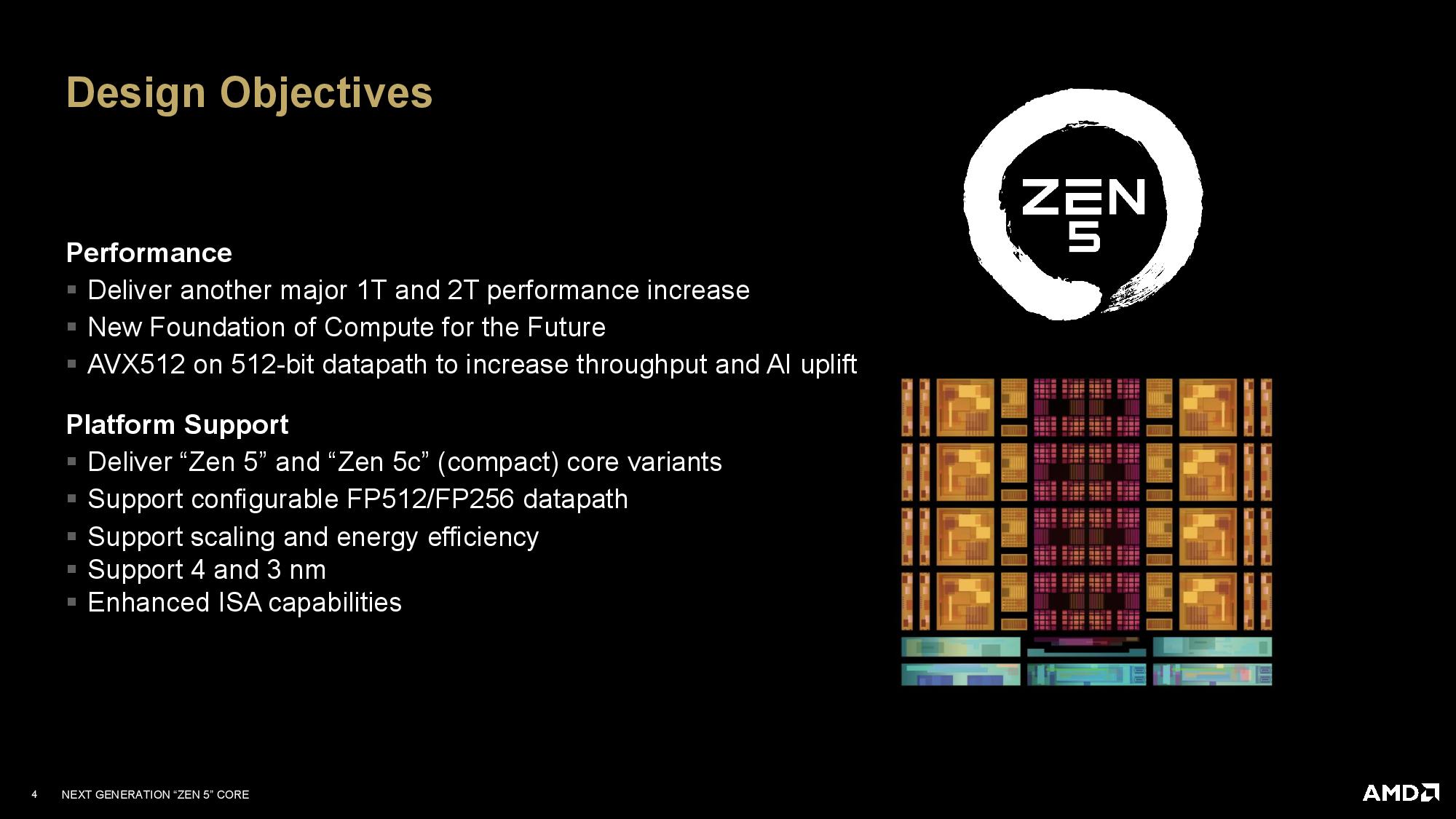
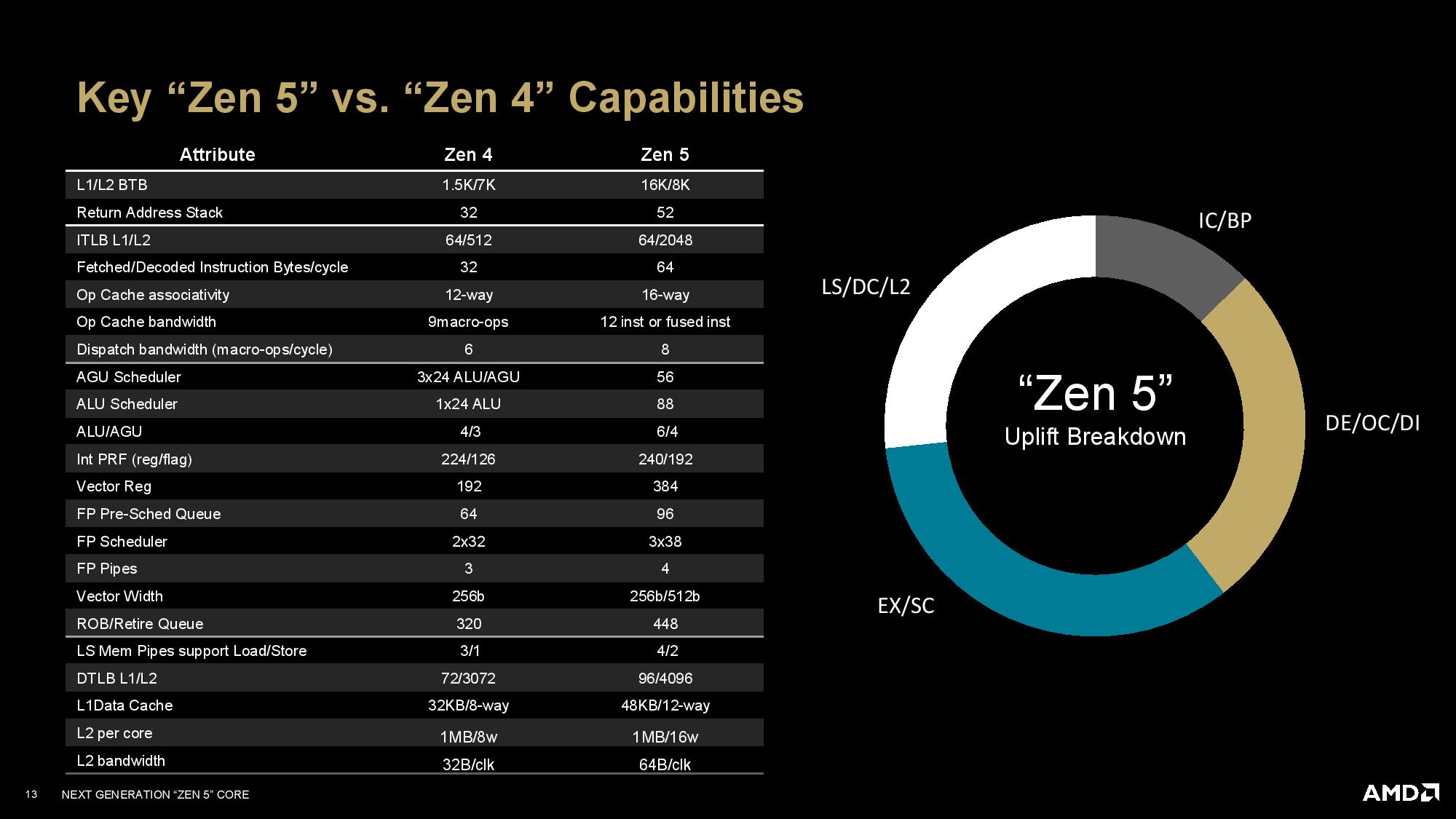
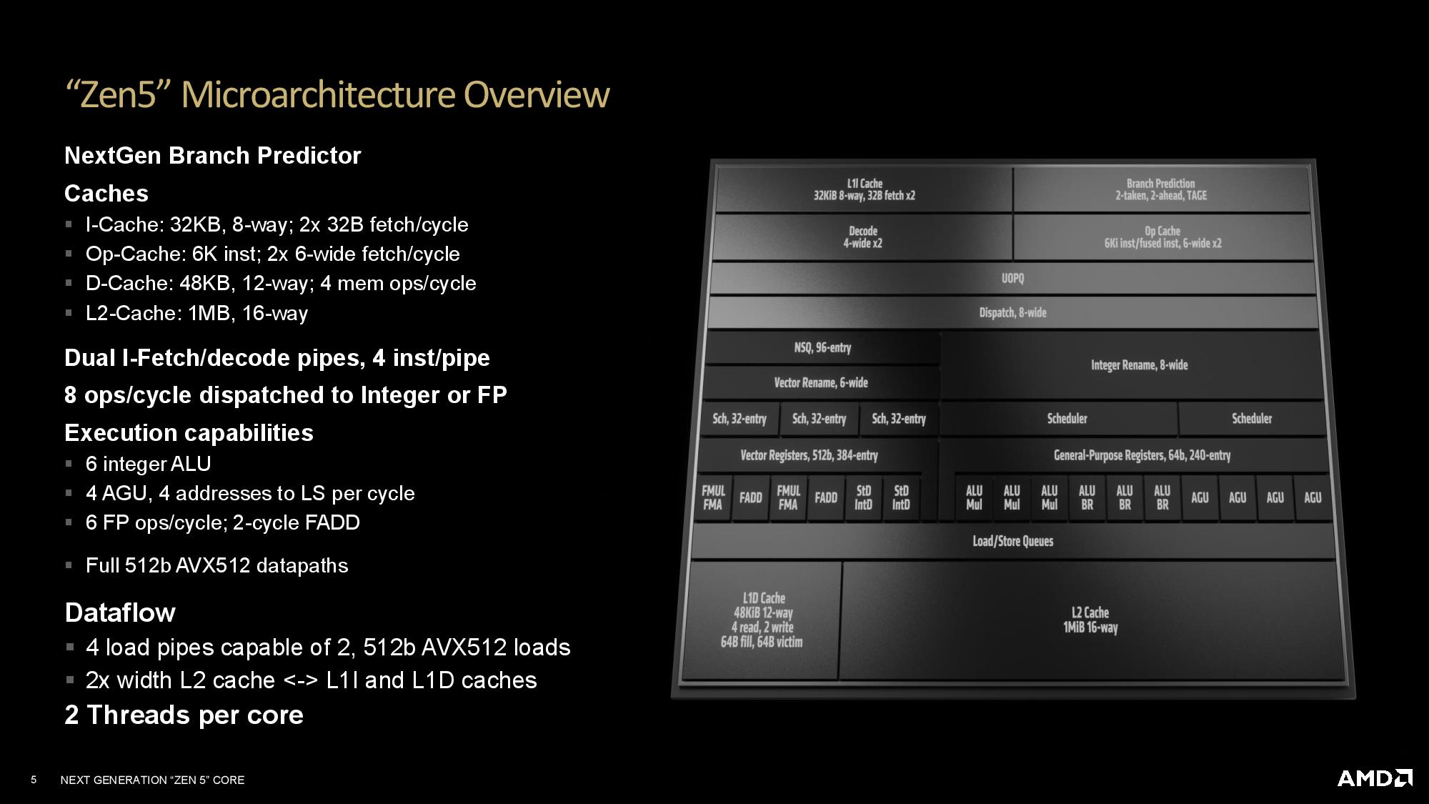
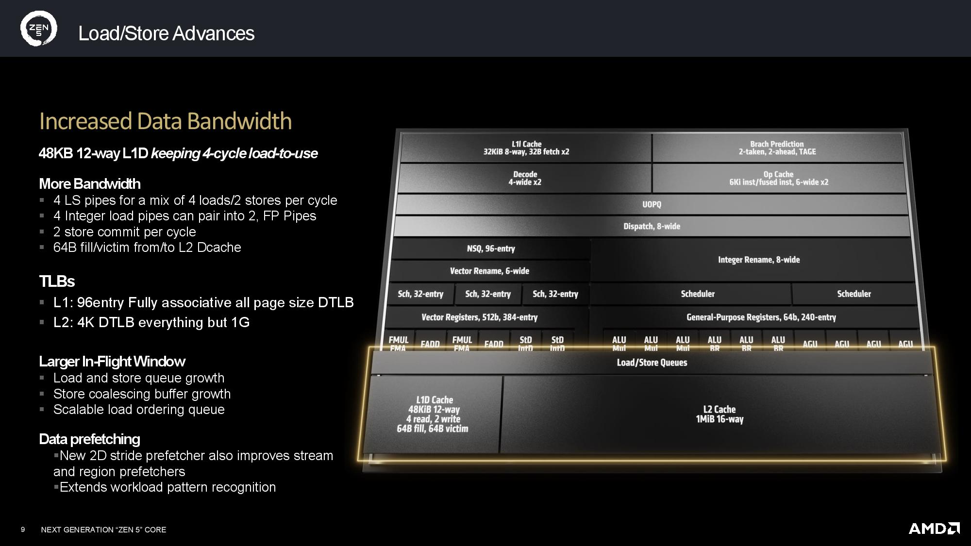
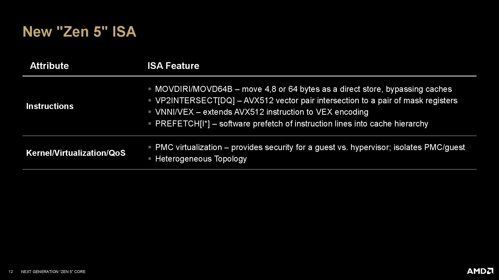
AMD has plumbed the Zen 5 architecture as a new foundation for computing, so it has several notable changes that will have far-reaching impacts as the company iterates with newer versions. Many of those features are outlined on the first slide that breaks down the most important changes over Zen 4. AMD also provided more detailed slides for the various components of the core and outlined the new ISA extensions supported with Zen 5.
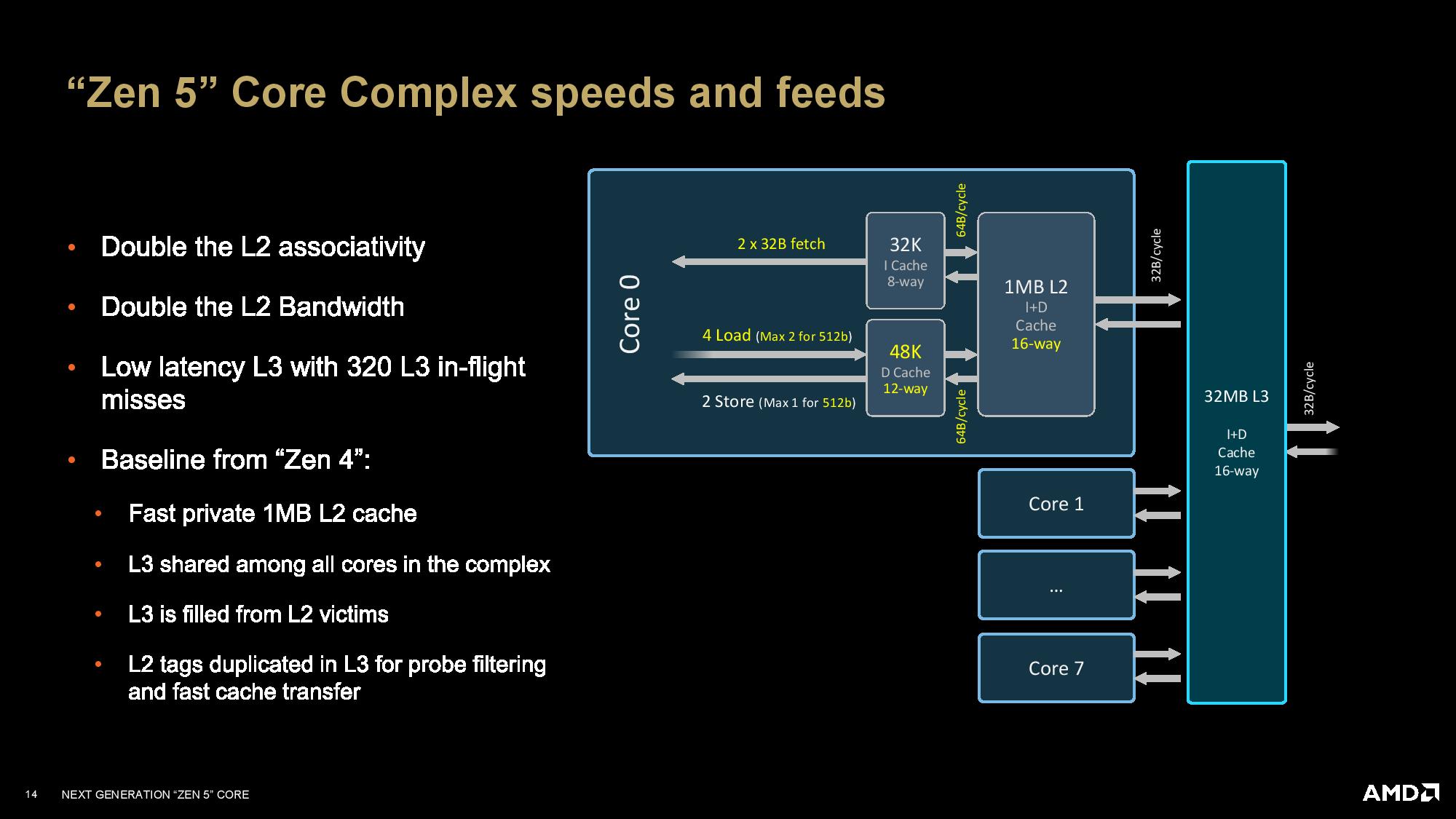
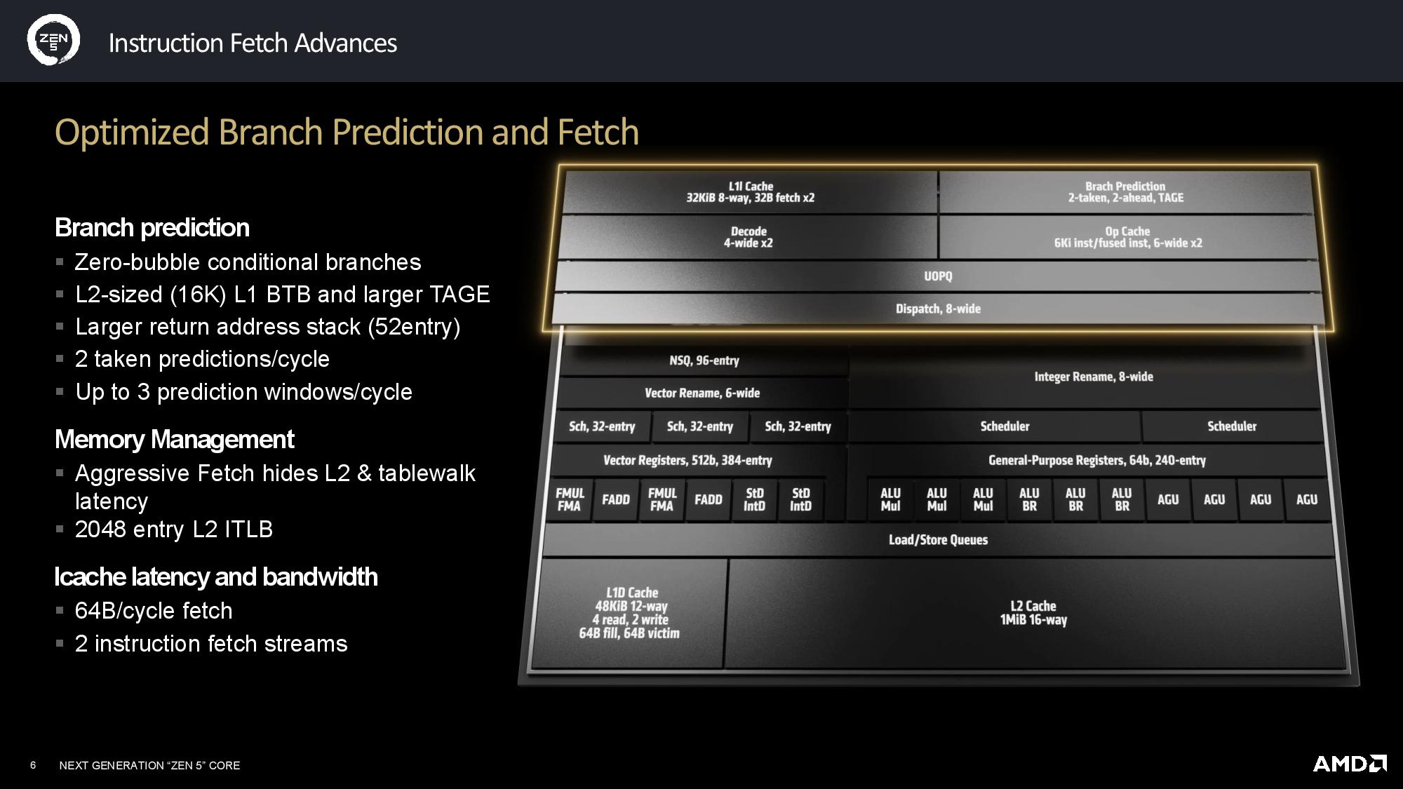
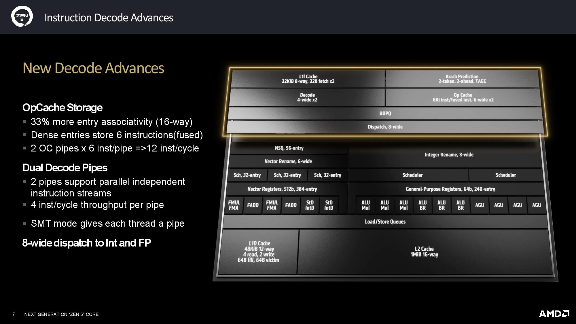
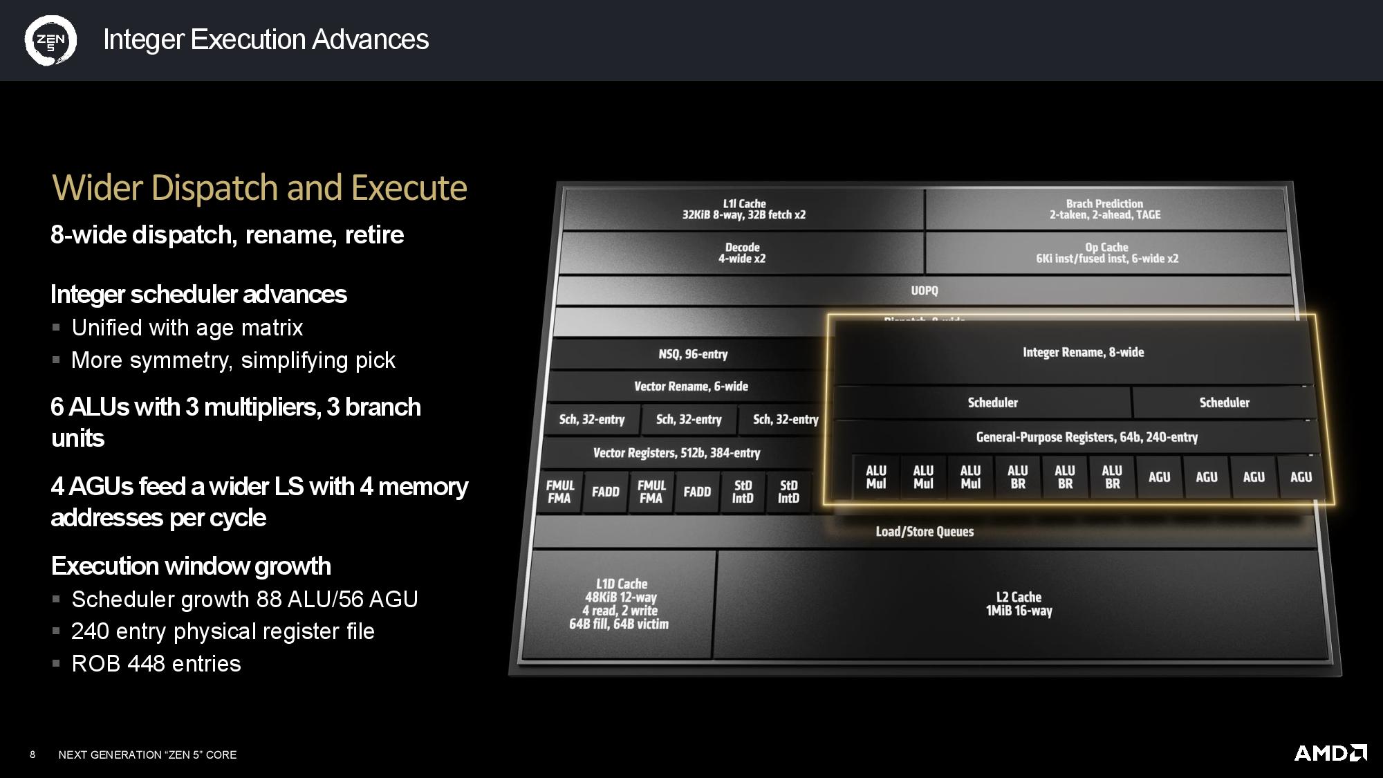
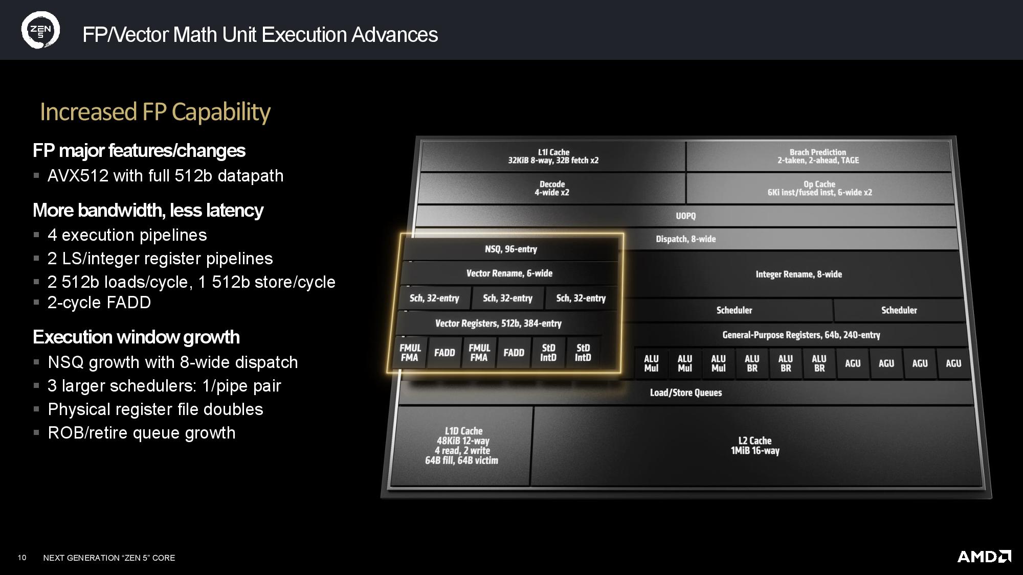
Due to time constraints, we'll provide the full write-up of the new microarchitectural details in our pending review. However, pay particular attention to the second slide (Zen 5 core complex speeds and feeds); this slide has new information about the connections between the different cache levels. We also learned that Zen 5's average misprediction latency has increased by one cycle (for reference, Zen 4 misprediction latency ranged between 12 to 18 cycles, with 13 cycles being a common latency).
Wrapping things up, the Zen 5-powered Ryzen 9000 'Granite Ridge' and Ryzen AI 300 'Strix Point' chips arrive July 31. If tradition holds, reviews will be posted then or the day before, though laptop availability will likely be less predictable than the desktop CPUs. Stay tuned for our full review, including the usual suite of benchmarks.