Space solar cells are evolving to address next generation deployments that require higher levels of performance, reliability, manufacturing scalability and cost. Prior generations used 4” and 6” Ge wafers to fabricate these solar cells. Increasingly, the focus is on using larger diameter substrates. Materials companies like Umicore have developed 8” Germanium wafers that have been evaluated for performance, purity and manufacturing scalability. The results are promising and highlight the time-honored maxim of the semiconductor industry - continue increasing wafer size as new applications emerge. Similar to solar cells, VCSELs are entering a phase where emerging applications are likely to challenge the current manufacturing platforms that rely on 6” GaAs substrates.
Apple’s deployment of a VCSEL (Vertical Cavity Surface Emitting Laser) based, world facing LiDAR on the iPad and iPhone platforms has significant impact on other applications like automotive LiDAR. There is a fundamental difference between consumer and automotive LiDAR applications. Smart phones typically do not demand high range, Field of View (FoV) or points per second (PPS), whereas automotive applications are geared toward safety and require significantly higher levels of performance and reliability. Consequently, VCSEL arrays in consumer applications tend to be smaller (1-2 mm²), whereas VCSEL based automotive LiDAR uses ~10X larger VCSEL sizes (10-30 mm²).
VCSELs were originally developed in the early part of this century for data communication and industrial sensing applications. They offered a lower cost alternative to edge emitting lasers (EELs) which are more expensive to fabricate at a semiconductor and packaging level. For the wavelengths used (typically 8XX-9XX nm), GaAs was the appropriate choice of semiconductor materials. The volumes were low and the size of the VCSEL die was <1 mm² per product, so 4” wafers were perfectly adequate.
As high volume consumer applications like smart phones using VCSEL arrays proliferated in the 2018 timeframe, higher volumes and the larger areas of semiconductors used drove a transition to larger wafer sizes (6” GaAs wafers). This was driven by capacity and cost constraints (generally, semiconductor processing costs do not increase dramatically with wafer size, enabling lower per unit costs as wafer size increases). 4” substrates provided ~4000 VCSELs per wafer, not enough to supply the millions of smart phones produced every year. 6” wafers yield about 10,000 VCSEL arrays/wafer. Moving to larger wafers is not trivial however. Re-tooling of semiconductor equipment is necessary (capital investment), higher wafer breakage costs could result (larger GaAs wafers are brittle and tend to break more easily with handling and processing stresses), and semiconductor processing has to be re-optimized (to guarantee good device quality across larger diameter wafers). After a significant amount of effort, this seems to have been accomplished by multiple suppliers like Lumentum, II-VI and others who have successfully designed in their GaAs VCSEL arrays into the current generation of smart phones.
The investments required by the supply chain to transition to a new material system and larger substrates can only be justified if:
- End customers and new applications demand significantly higher volumes, lower costs, higher performance and different features (market driver)
- The supply chain is able to conclusively demonstrate the ability to deliver these requirements (operational capability)
It is a chicken-and-egg problem - while the supply chain waits for assurance that customers will buy or fund the development, the customer base looks for proof to convince them of the benefits. Part 1 (this article) discusses the market aspect. Part 2 will discuss how the the supply chain is responding to these market demands.
Markets and Applications
From a demand and market perspective, automotive LiDAR, Augmented/Virtual Reality (AR/VR), and emerging smart glass applications are the prime drivers for a transition to larger semiconductor substrates in alternate material systems.
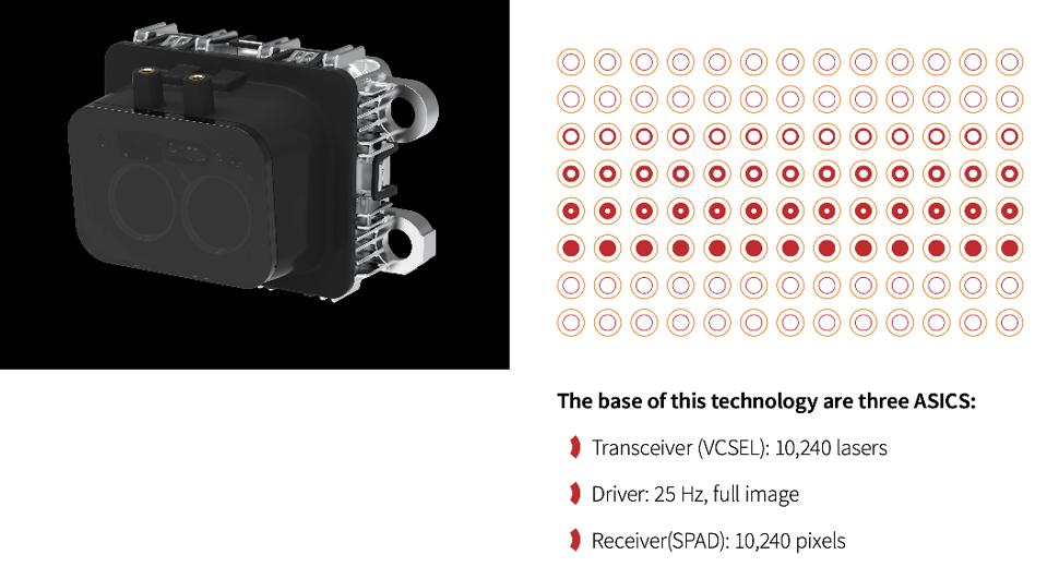
Ibeo, based in Hamburg, Germany, is one of the pioneers in LiDAR for automotive applications. The company was started in 1998, long before LiDAR became fashionable, exciting and sexy. It pioneered LiDAR applications to autonomous driving by participating in the 2007 DARPA Grand Challenge. Ibeo technology was also used in the Scala LiDAR product (owned by Valeo, a France based automotive Tier 1 supplier), a 4-beam, mechanically scanned system. Valeo successfully qualified this design in 2018, and is integrating it into L2 (Level 2) and L3 (Level 3) automation features in cars. IbeoNEXT is the next generation product (see Figure 2) - a solid state electronically scanned system that deploys 2D arrays of VCSELs and SPADs (Single Photon Avalanche Photodiodes).

ZF Friedrichshafen AG is an investor in Ibeo as well as a Tier 1 industrialization partner. The VCSELs are procured from AMS Technologies . The solid state construction is attractive from a reliability perspective, and the higher number of VCSEL emitters in the ~30 mm² array (~10,000) allows for higher resolution and range. IbeoNext has secured a design win into the upcoming models of Great Wall Motors, a leading Chinese automotive OEM. The large VCSEL area currently makes it one of the more expensive components in the LiDAR. Achieving lower price points (according to Ibeo, the future price target is $100 in quantities of a million units/year), will require VCSEL costs to reduce dramatically (by a factor of 5-10X). One way to do this is to increase the VCSEL power density (although this is constrained by eye-safety limits at the 8XX-9XX nm wavelengths the VCSELs operate at, as well as the ability to thermally manage the heat and prevent overheating). The other option is to move towards larger area substrates.
Michael Kiehn, Vice President of Advanced Engineering indicates that apart from the dramatically lower costs, other desirable features of next generation VCSELs include:
- Addressability: current construction of the VCSEL and interconnect schemes to the driver electronics allows row-level addressability. Ideally, region of interest (ROI) addressability is required, which means rectangular regions in the array should be addressable.
- Back-side illuminated VCSELs: allow for more uniform current distribution leading to higher VCSEL power and lifetimes. This requires a shift to 940 nm wavelengths and back-illuminated VCSELs.
- 3D integration of optical and electronic wafers: via flip chip or other interconnect platforms would provide wafer level packaging, and reduce device size, which is critical for consumer applications like smart phones and smart glasses (Ibeo also counts among its investors, AAC Technologies in China, which provides a variety of acoustic, haptic and optical sensors into these applications).
Ouster recently acquired Sense Photonics as part of its strategy to penetrate the automotive market with a solid state, flash LiDAR solution. Although both Ouster and Sense use VCSELs and SPADs, Sense is unique in that it is probably the only company capable of pure flash operation (similar to CMOS cameras) with no scanning (a global shutter solution where all pixels acquire data at the same time) and designed for long range performance.
According to Aravind Ratnam, (Head, Automotive Products), the flash LiDAR solution images to 200 m on 10% objects with 0.025° angular resolution. The LiDAR can be modified to work at shorter ranges with an expanded FoV by using alternative optics. Looking ahead, the VCSEL needs to evolve in terms of wavelength vs temperature drift, higher power density and cost. Increasing yields on the current 6” VCSEL manufacturing is one tool to achieve this. The other is to move to larger wafer diameters and different substrate material systems as long as they are demonstrated to have equal or better performance, yield and costs as the current approaches.
Opsys, based in Israel and California, focuses on VCSEL-based, solid state automotive scanning LiDAR. The company has been successful in design wins with major Chinese automotive OEM and Tier 1 customers, and has agreements in place with a major Korean automotive Tier 1 supplier. The base unit (expected production launch date is 2022) uses a total of 6,500 VCSEL apertures (~30 mm² chip size) to illuminate a ~14,000 pixel SPAD array, and is designed for long range, high resolution and high frame rates, while operating well below the FDA eye safety limit. Each unit uses low energy laser pulses at high pulse rates to achieve this performance. Modular construction for addressing varying customer requirements is enabled by combining multiple base units operating at different wavelengths (905 and 940 nm to prevent cross talk and enable high laser pulse rates).
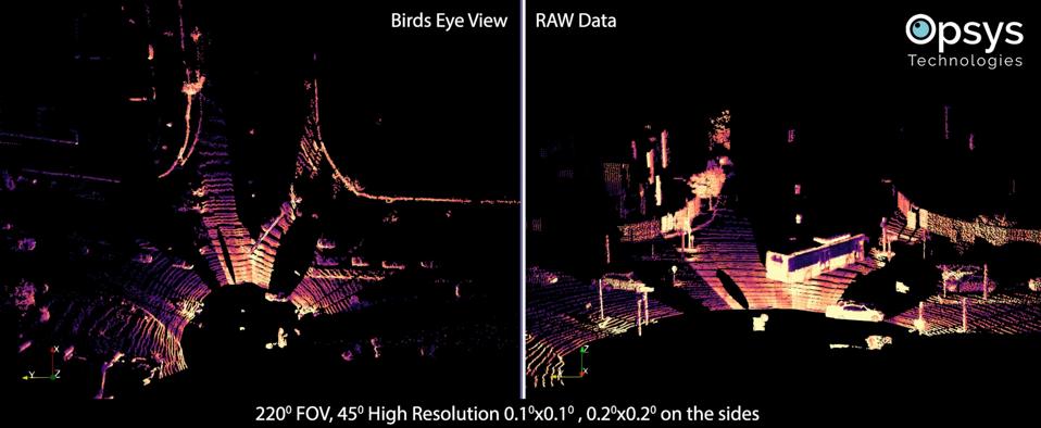
Figure 3 shows raw point cloud data (front and top views) created with 8 units to image a 220°x13° FoV for a particular automotive OEM customer. The center 45°x13° region uses four units providing a 0.1°x 0.1° angular resolution, and images to a 200 m range. Two units on each side cover a 90°x13° FoV with 0.2°x 0.2° angular resolution.

Per Eitan Gertel, Executive Chairman and founder of Opsys, a proprietary silicon driver ASIC will enable a fully addressable VCSEL and ROI imaging. This will lead to efficiencies in power management, data processing speeds, lower latency, high resolution, higher range and excellent POD performance. In terms of VCSEL needs going forward, the ability to do ROI imaging and a factor of 3X reduction in costs are critical. Moving to larger VCSEL substrate diameters is one path to achieving the cost targets.
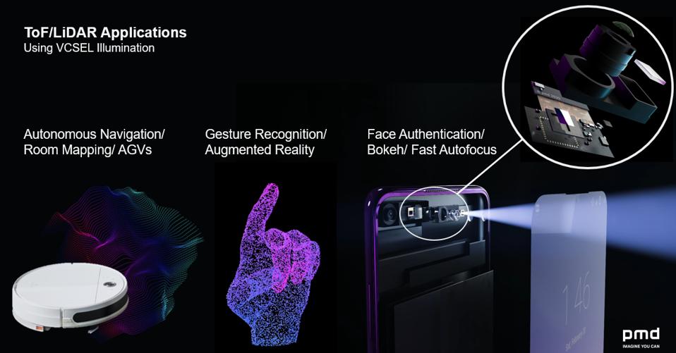
pmdtechnologies AG, based in Siegen, Germany is a leading supplier of short range LiDAR into consumer devices and augmented reality applications. It uses a VCSEL array as part of the LiDAR along with a specially designed VGA format infrared CMOS imager. lnfineon and pmdtechnologies collaborated to release the first generation of the REAL3™ image sensor in 2015 (currently at its sixth generation of productization). Applications (see Figure 4) include consumer mobile and AR/VR (room scanning, gesture control, bokeh effects and fast autofocus), industrial (automation, surveillance and robotics) and automotive (in-cabin passenger alertness monitoring, as well as road-facing).

In 2016, REAL3™ was designed into Google’s
- Cost & Manufacturing Capacity: as 3D imagers proliferate in lower priced consumer devices, VCSEL costs need to constantly reduce, and manufacturing capacity needs to increase.
- Higher speed operation: the ability to operate the VCSEL at higher speeds is important for dynamic scenes and safety applications
- VCSEL Addressability: current interconnect schemes make it impractical to operate the VCSEL to support adaptive, ROI imaging. Next generation VCSELs need to address this.
- Green Fabrication: GaAs substrate based processes are not compatible with recycling processes. Currently, regulatory bodies accommodate this constraint, although this is liable to change in the future.
- Wafer level integration of VCSEL and driver electronics: traditional opto-electronics relies on discrete integration of the optical and electronic semiconductors. Wafer level integration in a CMOS environment would help reduce costs, and lead to smaller devices
- Chip scale LiDAR: Ideally, if wafer level integration were possible, one could envision a complete LiDAR system on a chip which is critical from a size and integration perspective.
AR and other applications built into smart glasses are also a new emerging application, driving diverse applications from gaming, education and training, remote expert support and manufacturing operations. Mercedes and Microsoft are working on HoloLens smart glasses to equip dealerships with the ability to perform complex repairs using remote support - saving on time and money. LG Innotek (based in Korea) is supplying the current VCSEL based LiDAR modules for the Apple iPod and iPhone, and is reportedly preparing to supply such modules to Apple and Microsoft for VR/AR smart glasses. Vuzix (VUZI), a Rochester, New York based smart glass manufacturer believes that embedding LiDAR into smart glasses will drive significant applications ranging from medicine, construction and oil exploration to law enforcement and remote expert assistance. VCSEL based LiDARs are best suited for integration into these platforms (similar to smart phones), and will need to be power efficient and low cost in order to scale these applications.
Exciting applications await VCSEL-based LiDAR. Customers are clear about how they need VCSELs to improve in terms of cost, capacity, performance and features going forward. Part 2 of this article will explore how the supply chain is responding to these challenges.


