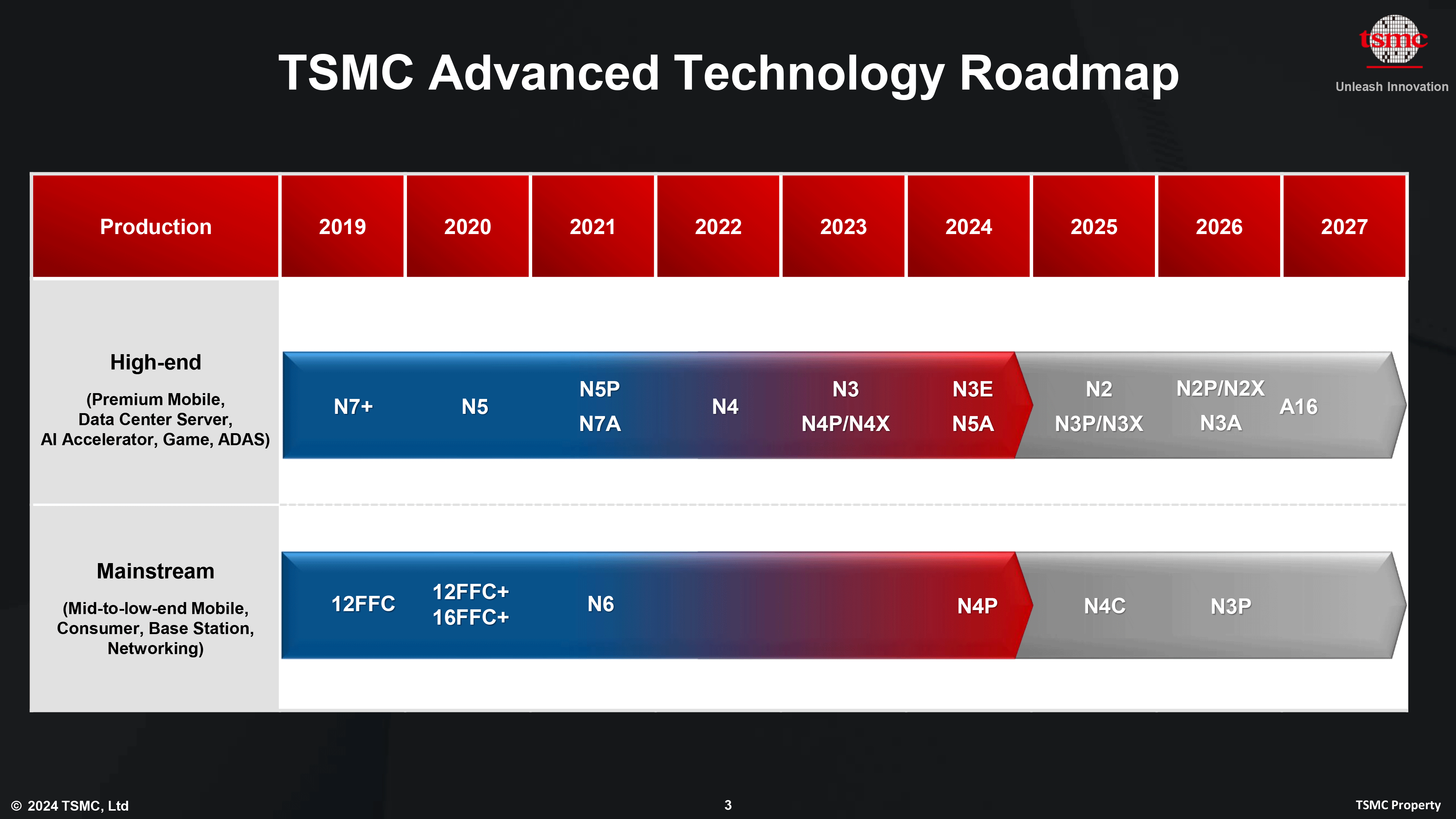
At the North American Technology Symposium 2024, TSMC detailed its progress and plans for its 2nm technology nodes, including the innovative NanoFlex technology. Just as TSMC planned, the company will start mass production of chips on its N2 process technology in the second half of 2025. Meanwhile, TSMC's N2P — the company's 2nd Generation 2nm-class node — will not offer a backside power delivery network. However, 2nm nodes will still feature improved power circuitry compared to 3nm processes.
TSMC's forthcoming N2 manufacturing technology promises significant advancements over existing N3E fabrication processes, with expected performance boosts of 10% to 15% and a reduction in power consumption by 25% to 30%. Additionally, the transition to the N2 node is projected to increase chip density by approximately 1.15 times, a significant improvement. In total, TSMC's N2 family is expected to include at least three nodes: vanilla N2, performance-enhanced N2P, and HPC-oriented N2X.
All of TSMC's N2 process technologies will rely on gate-all-around (GAA) nanosheet transistors that allow chipmakers to increase channel width for increased performance or reduce it to lower power consumption. This gives both chip designers and fabs quite a lot of flexibility, but TSMC goes one step further with its N2 family and its NanoFlex technology.
NanoFlex allows chip designers to mix and match standard cells from various libraries (high-performance, low-power, high-density) within the same block, optimizing chip performance, power, and area characteristics. TSMC's N3 production nodes already support FinFlex technology, providing similar capabilities, but things work a lot differently with GAA nanosheet transistors for obvious reasons. TSMC says that we can expect up to 15% higher performance with tailored designs, though this is, of course, the best-case scenario.
However, TSMC has revised some of the features of its N2P fabrication technology. Contrary to prior announcements, N2P will not incorporate a backside power delivery network, opting instead for conventional power delivery mechanisms. This decision redirects the integration of such advanced power delivery to future generation nodes, particularly A16 and A14.
Another major enhancement in the N2 node is the integration of a super-high-performance metal-insulator-metal (SHPMIM) capacitor. This new capacitor boasts more than double the capacity density and reduces both sheet and via resistance by 50%, compared to its predecessor, the super-high-density metal-insulator-metal (SHDMIM) capacitor introduced several years ago. The introduction of SHPMIM will greatly improve the stability of power delivery, which will optimize performance and power consumption.
In general, TSMC's N2 is on track, and with A16 set to coexist with N2P, the company will have several quite competitive offerings in the coming years.