TSMC is on track to mass produce the first chips on its A16 (1.6nm-class) process technology in late 2016, the company announced at its European Open Innovation Platform (OIP) Ecosystem Forum in Amsterdam, the Netherlands, earlier this week. The new production node features TSMC's Super Power Rail (SPR) backside power delivery network (BSPDN), which enables enhanced power delivery, which routes all power through the back side of the chip, and higher transistor density. But while this BSPDN solves some challenges, it adds others, so additional design efforts are required.
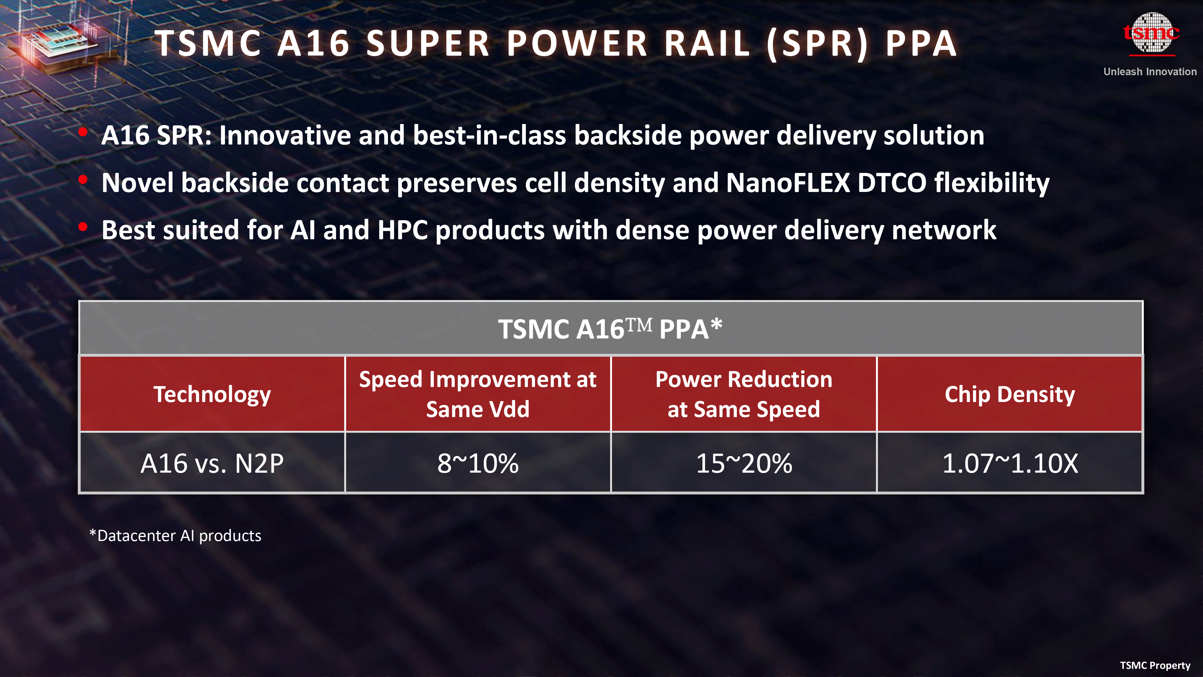
TSMC's A16 process will use gate-all-around (GAAFET) nanosheet transistors with an architecture similar to those featured by TSMC's N2-series process technologies (2nm-class) and include a backside power rail to enhance power delivery and boost transistor density. Compared to the N2P fabrication technology, A16 promises an 8%-10% performance gain at the same voltage and complexity or a 15%-20% power reduction at the same frequency and transistor count. In addition, TSMC estimates a 1.07x to 1.10x increase in chip density for high-end AI processors, depending on transistor types and libraries used.

Architecturally, A16 transistors are similar to N2 transistors, according to Ken Wang, TSMC's director of design solution exploration and tech benchmarking division. This simplifies migration to this process technology from N2.
"The logic layout migration from N2P to A16 is actually quite straightforward because the cell structure and most of the layout patterns are quite the same," said Wang. "So, besides keeping the same front side structure, the beauty of A16 is that it inherits the NanoFlex feature from N2 device width modulation for the maximum driving strength."
TSMC's Super Power Rail connects the backside power delivery network directly to each transistor's source and drain through a specialized contact, minimizing wire length and resistance to maximize performance and power efficiency. Production-wise, this implementation is among the most intricate BSPDN designs, surpassing the complexity of Intel's Power Via.

However, advanced BSPDN implementation also means that chip designers must completely redesign their power delivery network, route it in a new way, and, therefore, apply new place-and-route strategies, which is to be expected. Also, they have to do some thermal mitigation because hot spots of the chip will now be located under a set of wires, making heat dissipation harder.
Designing chips with a backside PDN essentially means adopting new implementation methods as many things change, including the design flow itself. Wang mentioned the usage of new thermal aware place-and-route software, new clock tree construction, different IR-Drop analysis, dissimilar power domains, and different thermal analysis sign-off, among others.
Considering the new implementation flow, new versions of EDA tools and simulation software are required. Since we're talking about a node similar to TSMC's N2, many things are ready, albeit in a pre-0.5 version of EDA tools from leading makers like Cadence and Synopsys.
"A16 is a technology suited for designs with complex routes and dense PDN," said Wang. "However, it also creates new challenges, so additional design effort is needed. Our backside contact VB also needs complete silicon validation with diligence. In the meantime, we have a comprehensive A16 EDA enablement program, which is ongoing, and we will continue to update the A16 EDA status."


