TSMC disclosed major roadmap updates for its N3 (3-nanometer class) family of process technologies at its 2023 North American Technology Symposium this week. As TSMC's final high-performance node based on FinFET transistors, N3 will last for many years and will include multiple versions, including N3P, a performance-enhancing optical shrink of N3E, and performance-focused N3X for HPC applications that tolerate high leakage and power.
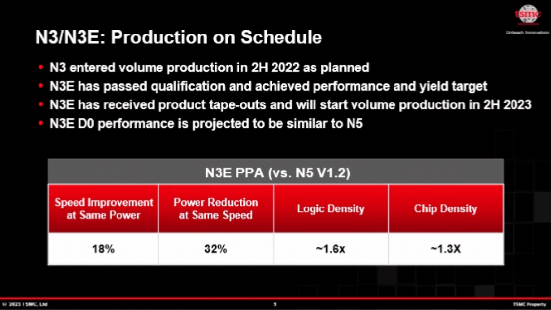
TSMC's mass production on its N3 (also known as N3B) process technology is already underway, but this node uses extreme ultraviolet lithography on up to 25 layers and can even use EUV double patterning, which makes it a particular expensive node to use. As a result, TSMC expects the majority of its clients to use N3E, which can use EUV on up to 19 layers, does not use double patterning EUV, has a wider process window, and better yields. N3E, which will be used for high volume manufacturing in H2 2023, will also be the base for TSMC's further 3nm evolution.

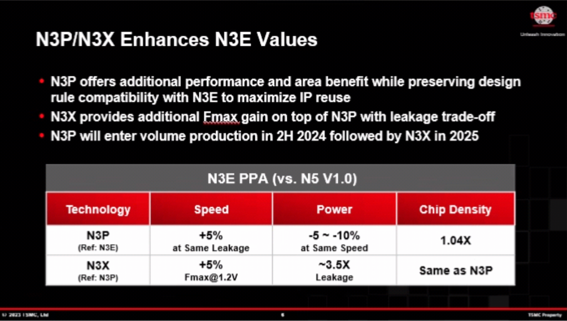
The first step in that evolution will be N3P. This technology will largely be an optical shrink of N3E that will feature some other refinements enabling a 5% performance boost at the same leakage, a 5% to 10% power reduction at the same clocks, and a 4% higher transistor density for a 'mixed' chip consisting of 50% logic, 30% SRAM, and 20% analog circuits.
As an optical shrink of N3E, N3P preserves its design rules, allowing chip designers to reuse N3E IP on the new node. This is rather important as IP design companies like Ansys, Cadence, and Synopsys already have a lot of IP aimed at N3E chips. Meanwhile, optical shrink implies on density improvements for all kinds of transistors and circuits, including SRAM, a type of circuits that has struggled to shrink in the recent years (something particularly bad for modern SRAM-intensive designs). N3P will be ready for mass production in 2024.

Following N3P, TSMC plans to further expand its N3 family and branch it into high-performance computing applications like CPUs and GPUs with N3X. This fabrication process is projected to provide at least 5% higher frequencies compared to N3P and also allow considerably higher voltages, which will further increase clocks at the cost of higher overall leakage.
TSMC asserts that its N3X node can handle at least 1.2V, a notably high voltage for a 3nm-class manufacturing technology. This comes with a considerable trade-off, as TSMC anticipates a staggering 250% increase in power leakage compared to N3P. This highlights that N3X is primarily suited for HPC CPUs and will require chip designers to exercise caution when developing their highest performance power hungry chips, such as datacenter CPUs and compute GPUs.
In terms of transistor density, N3X will match N3P's capabilities. TSMC has not specified whether its N3P and N3E will have compatible design rules, leaving room for intrigue about whether designs can be ported between the two nodes.


