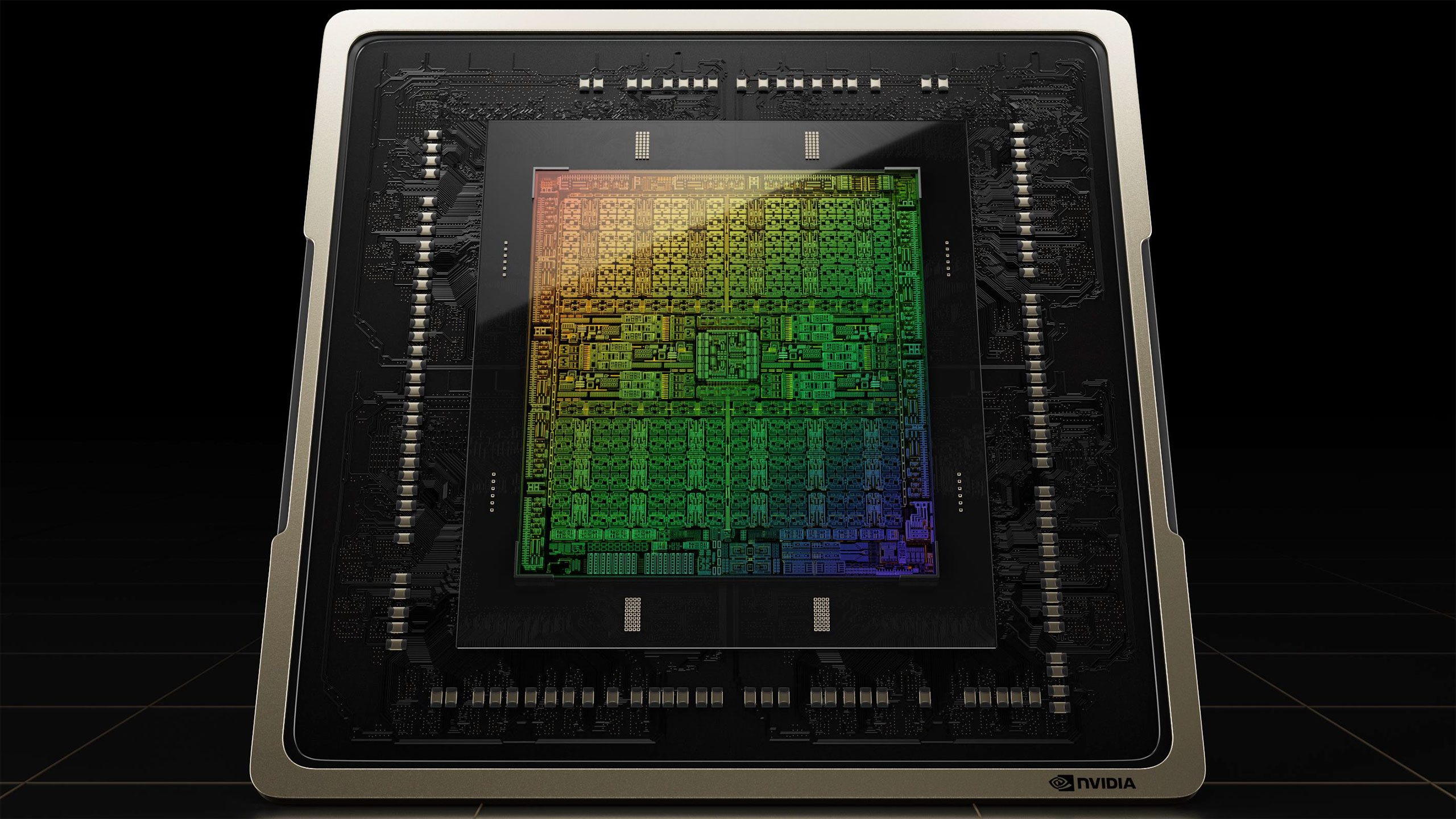
Nvidia's RTX 5090 will undoubtedly be a powerhouse GPU, and part of the reason for that will be the enormous GB202 chip powering it that allegedly comes in at an 744mm-squared, according to renowned hardware leaker MEGAsizeGPU at X. If the leak proves correct, the RTX 5090's die size sees a sizeable bump 22% bump compared to the RTX 4090's AD102 GPU. That would likely drive prices up — both for Nvidia and the end-customers.
The Nvidia Blackwell RTX 50-series desktop GPUs are rumored to utilize TSMC's 4NP process (5nm), which is an enhanced version of the 4N used with the Ada Lovelace architecture (RTX 40-series). This process node is expected to offer a nice 30% bump in density, but that might not be fully accurate for the RTX 50 series. Regardless, a 744mm-squared die size is nearing reticle size limits (around 850mm^2).
To counteract this exact limitation, Nvidia employed a multi-chiplet design in its data center Blackwell B200 chips, but that notion apparently isn't viable for desktops given the high packaging costs and whatnot.
As per the tipster, the RTX 5090's GB202 GPU spans 744mm-squared (24mm x 31mm), while the entire package comes in at 3528mm-squared (64mm x 56mm). Package sizes aren't as important since they include the die itself along with capacitors, resistors, and other structural materials. In any case, the RTX 5090 will be the largest consumer GPU (in terms of die size) that we've seen since 2018. Turing manages to retain its crown since the TU102 (RTX 2080 Ti) GPU is just 10mm^2 larger than the GB202, per this leak.
Nvidia always builds some redundancy into its GPUs, so the top-end RTX 5090 solution likely doesn't use a fully enabled die. 'Prime' chips where the full-fat die works will typically get reserved for data center and professional GPUs. The fully-enabled GB202 chip allegedly offers 192 SMs and going by current leaks, with the RTX 5090 having an 88% enabled GB202 die (170 SMs).
That matches up perfectly with the RTX 4090, which was also limited to 88% (128 out of 144 SMs). The RTX 5080, per reports, sees a heavy nerf, with just 84 SMs so, die sizes could be roughly half as large as GB202. Nvidia will most probably incur heavy manufacturing costs for the RTX 5090, but that will invariably get passed down to the end customer. We expect to see a very large price delta between the 80-class and 90-class Blackwell cards.
A recent leak claims that Jensen Huang will debut Nvidia's flagship RTX 5090 and RTX 5080 GPUs at CES 2025. Afterward, mainstream RTX 5070 and 5070 Ti GPUs are expected sometime later during the first quarter, followed by the budget RTX 5060 offerings.


