HBM's future isn't just bright: it's also lightspeed, ultra-bandwidth, and super low-power. At this year's Open Compute Project (OCP) Global Summit, Samsung's Advanced Packaging Team Yan Li presented us with a glance at a more integrated future than we might expect: one where thermal and transistor density issues with further High Bandwidth Memory (HBM) development could be solved through photonics.
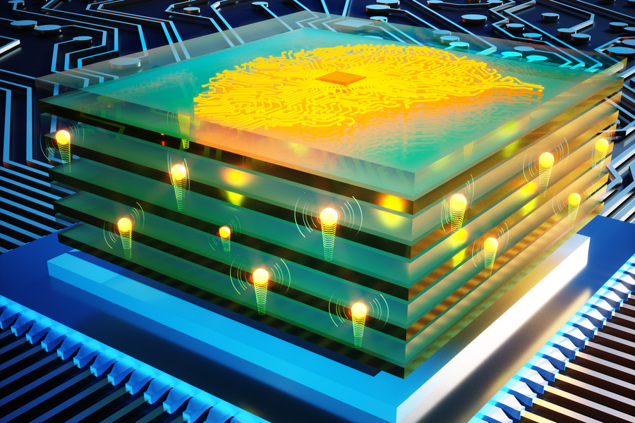
Photonics is based on a technology that can encode information on single photons (particles/waves of light), which means that it improves (almost) everything we care about in our current computing environment. There's both incredibly reduced power consumption (you're beaming particles of light instead of a flow of electrons) and improved processing speeds (with latencies achieving femtoseconds and propagation speed, well, approaching the lightspeed limit). Getting there is just a matter of engineering, quantum physics, and human ingenuity.
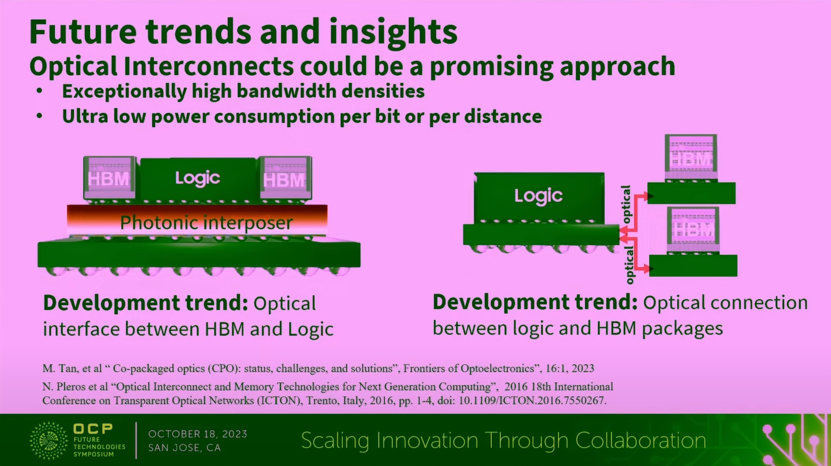
As it stands, the industry has made recognizable inroads in integrating photonics and HBM via two methods. One sees a photonics interposer being sandwiched between the base packaging layer and a top layer holding both logic (a GPU, for instance) and HBM itself, serving as the communications layer between them. This future seems expensive – there's the need for that interposer, as well as the need for both local logic and HBM to be configured with photonics I/O as well.
Another approach is to decouple the HBM memory banks from the chip package entirely. Instead of dealing with the chip packaging complexities (including logistics) of dealing with an interposer, you shift the HBM banks away from the chiplet itself and connect them (via photonics) to the logic. This simplifies chip manufacturing and packaging costs for both HBM and logic and does away with complex, in-circuitry, local conversion from digital to optical.
From this vantage point, that approach sounds most sensible. But then, it also means a deeper rethinking of server specifications and would also likely result in "HBM memory cubes" being a thing - HBM memory banks pre-loaded onto a specified photonics interface. Because you've decoupled HBM from the chip itself, and assuming you keep a standard optical communications interface, you can then look at an "upgradeable" product - one that's handled as if it were a stick of the best RAM kits.
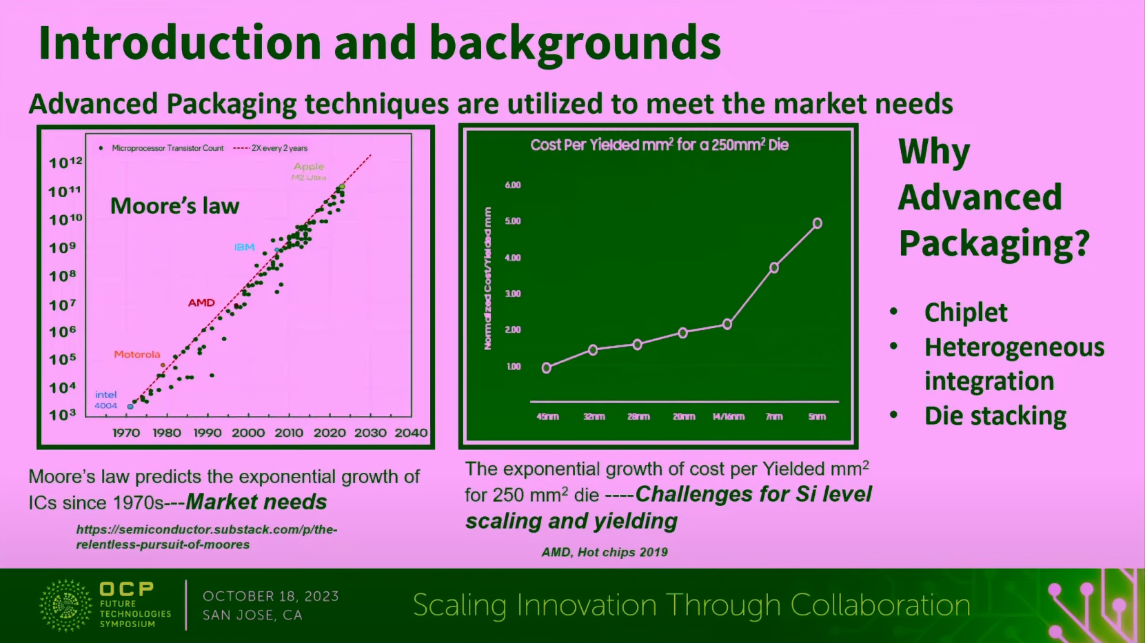
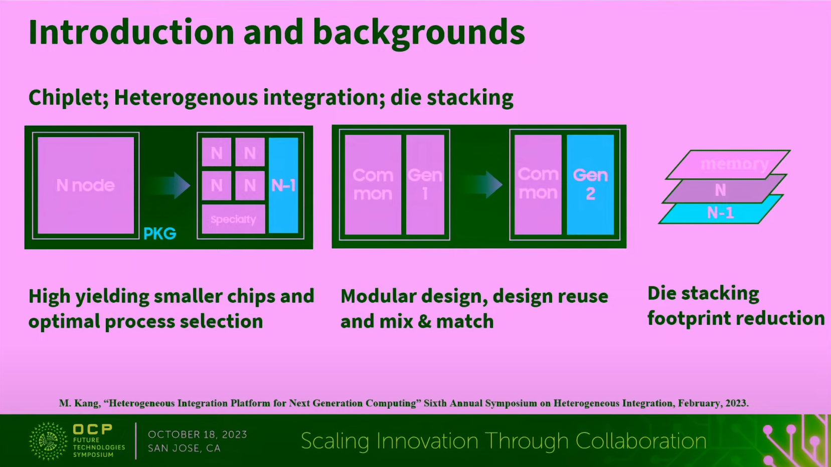
The presentation also goes into additional details on Samsung's HBM packaging, which is already offered in 2.5D and 3D solutions, and presents a brief overview of the racing horses that are Moore's Law and the increasing costs of semiconductor miniaturization in order to explain why photonics is indeed a part of our future. How far away into the future is hard to tell, but the road disappears far into it.