Although Chinese companies can no longer get advanced chipmaking tools from American, Japanese, or Dutch companies, they can still get advanced fab equipment from South Korean companies. A case in point is Nextin, a South Korean maker of optical wafer inspection equipment, which is expanding its presence in the Chinese semiconductor market, according to DigiTimes and The Elec reports.
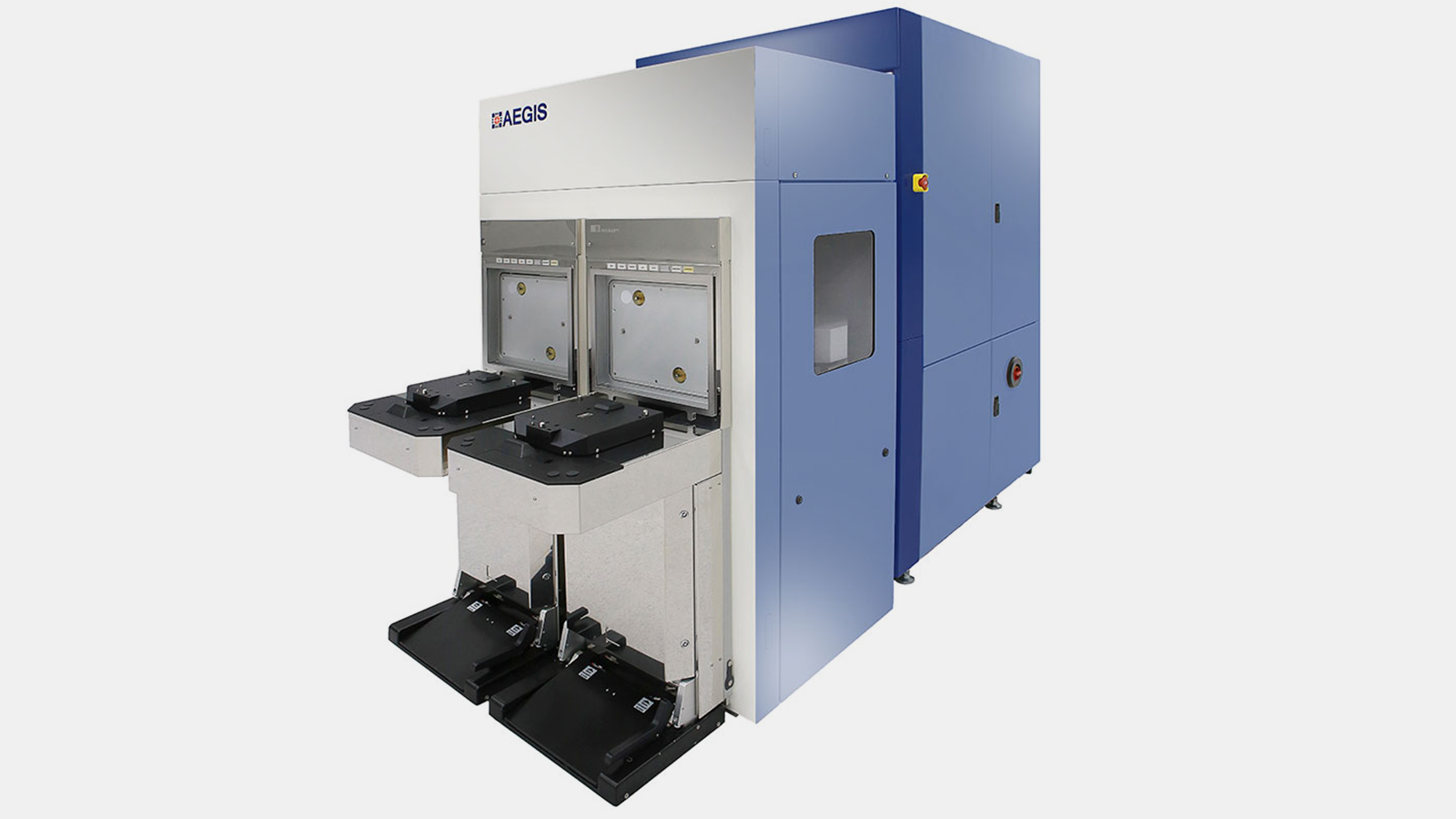
Nextin is said to have signed a deal with an undisclosed Chinese client for KRW7 billion ($5.39 million) for one Aegis 3 machine, according to DigiTimes. This model is claimed to offer 30% faster inspection speeds compared to the Aegis 2, and a computing performance of 1.47 TFLOPS .
Nextin is reportedly supplying optical inspection tools not only to SK Hynix China, but also to the blacklisted Yangtze Memory Technologies (YMTC), and Semiconductor Manufacturing International Corporation (SMIC), says the source. YMTC and SMIC are backlisted by the U.S. Department of Commerce, no American technology can be supplied to them. Meanwhile, it is unclear whether Nextin continues to use U.S.-originated technology for products it ships to Chinese entities.
Optical inspection tools are meant to rapidly detect issues on wafers using bright-field (obtaining images through reflected light) and/or dark-field (using scattered light for detection) modes. Nextin's Aegis equipment can inspect both 200-mm and 300-mm wafers, as well as operate in both bright-field and dark-field modes. The bright-field method, which uses reflected light, can spot defects as tiny as 15nm. Meanwhile, the dark-field method, which relies on scattered light, can detect defects up to 30nm.
While Nextin's Aegis tool resolutions may not sound impressive by today's standards, defects do not have to be as small as the feature size to impact the functionality of the device. A defect that is 15nm in size can still significantly disrupt or impair the operation of structures in a 14nm or 7nm production node, making its detection crucial. Keeping in mind that optical detection tools are faster than e-beam or multi e-beam tools, these optical inspection tools are widely used today. For which fabs? The client decides. They also may not just be fabs, but storage facilities where they can be taken with no questions asked.
There are indications that Nextin is also investing more in the Chinese market in general. The company is reportedly pouring in $200 million into a project in Wuxi High-tech Zone and Wuxi Industrial Development Group to create an advanced manufacturing and R&D base for inspection detection equipment.