SanDisk on Wednesday introduced an interesting new memory that could wed the capacity of 3D NAND and the extreme bandwidth enabled by high bandwidth memory (HBM). SanDisk's high-bandwidth flash (HBF) memory enables access to multiple high-capacity 3D NAND arrays in parallel, thus providing plenty of bandwidth and capacity. The company positions HBF as a solution for AI inference applications that require high bandwidth and capacity coupled with low power requirements. The first-generation HBF can enable up to 4TB of VRAM capacity on a GPU, and more capacity in future revisions. SanDisk also foresees this tech making its way to cellphones and other types of devices. The company hasn't announced a release date yet.
"We are calling it the HBF technology to augment HBM memory for AI inference workloads," said Alper Ilkbahar, memory technology chief at SanDisk. "We are going to match the bandwidth of HBM memory while delivering 8 to 16 times capacity at a similar cost point."
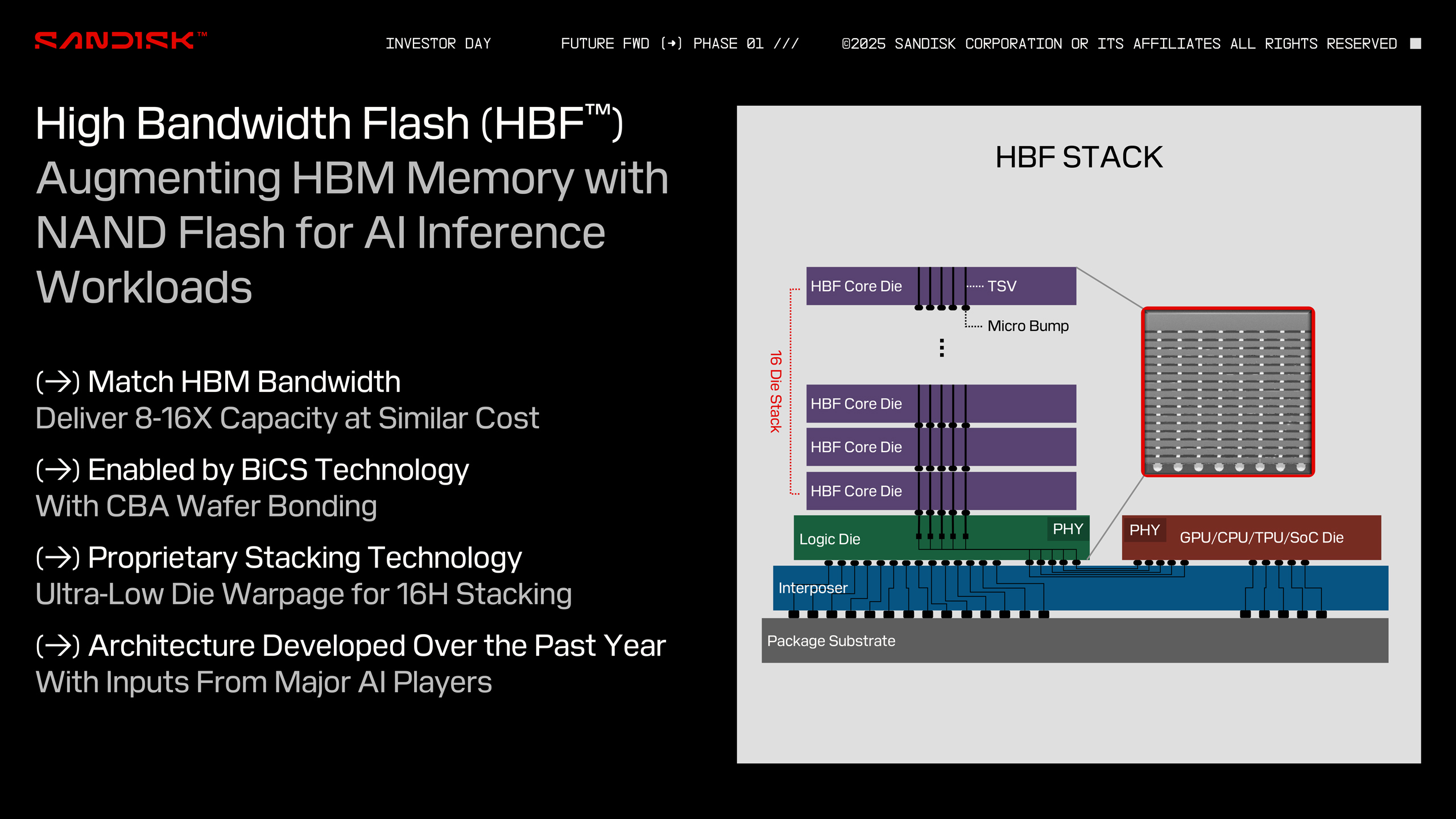
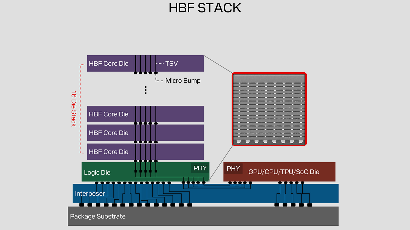
Conceptually, HBF is similar to HBM. It stacks multiple high-capacity, high-performance flash core dies interconnected using through-silicon vias (TSVs) on top of a logic die that can access flash arrays (or rather flash sub-arrays) in parallel. The underlying architecture of HBF is SanDisk's BICS 3D NAND using the CMOS directly bonded to Array (CBA) design that bonds a 3D NAND memory array on top of an I/O die made using logic process technology. That logic may be a key to enabling HBF.
"We challenged our engineers and said, what else could you do with this power of scaling," said Alper Ilkbahar. "The answer they came up with […] was moving to an architecture where we divide up this massive array into many, many arrays and access each of these arrays in parallel. When you do that, you get massive amounts of bandwidth. Now, what can we build with this? We are going to build high bandwidth flash."
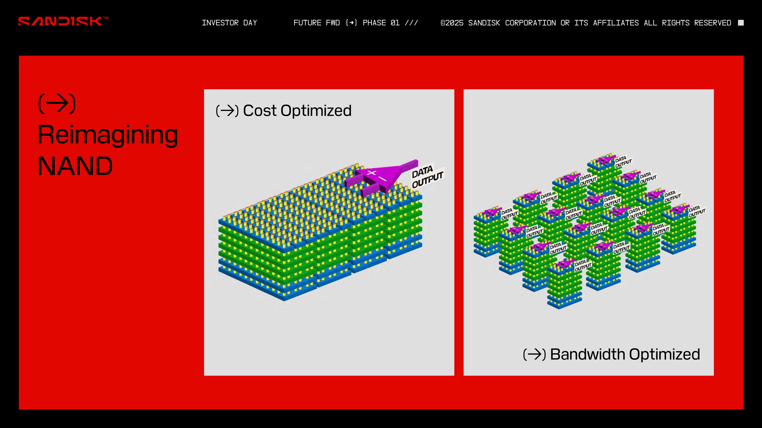
Traditional NAND die designs often treat the core NAND flash memory array as planes, pages, and blocks. A block is the smallest erasable area, and a page is the smallest writable area. HBF seems to break the die into 'many, many arrays' so they can be accessed concurrently. Each sub-array (with its own pages and blocks) presumably has its own dedicated read/write path. While this resembles how multi-plane NAND devices work, the HBF concept seems to go far beyond them.
For now, SanDisk says that its 1st-Gen HBF will use 16 HBF core dies. To enable such devices, SanDisk says that it has invented a proprietary stacking technology that features minimal warpage to enable stacking 16 HBF core dies, and a logic die that can simultaneously access data from multiple HBF core dies. The complexity of logic that can handle hundreds or thousands of concurrent data streams should be higher than that of a typical SSD controller.
Unfortunately, SanDisk does not disclose the actual performance numbers of its HBF products, so we can only wonder whether HBF matches the per-stack performance of the original HBM (~ 128 GB/s) or the shiny new HBM3E, which provides 1 TB/s per stack in the case of Nvidia's B200.
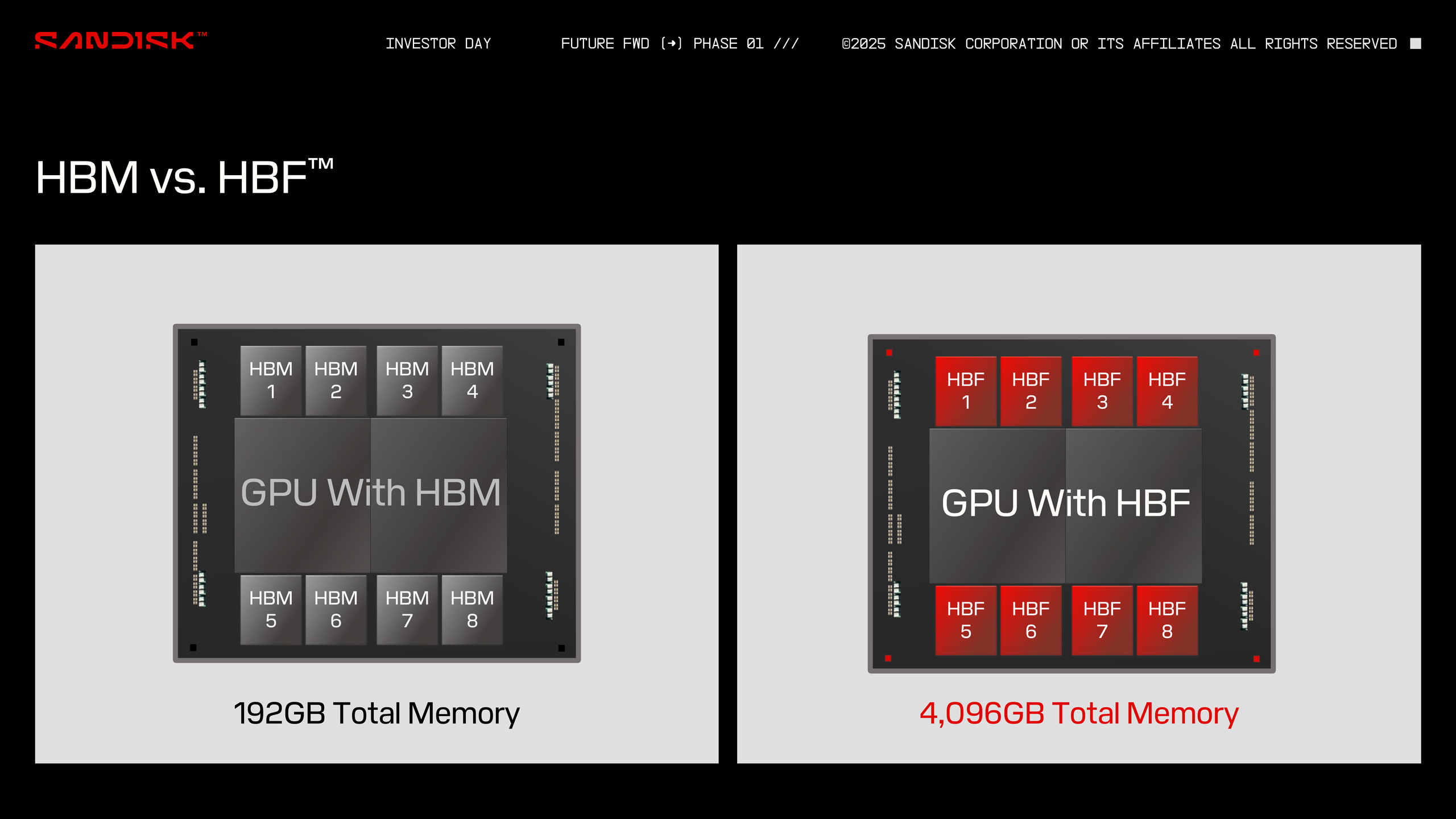
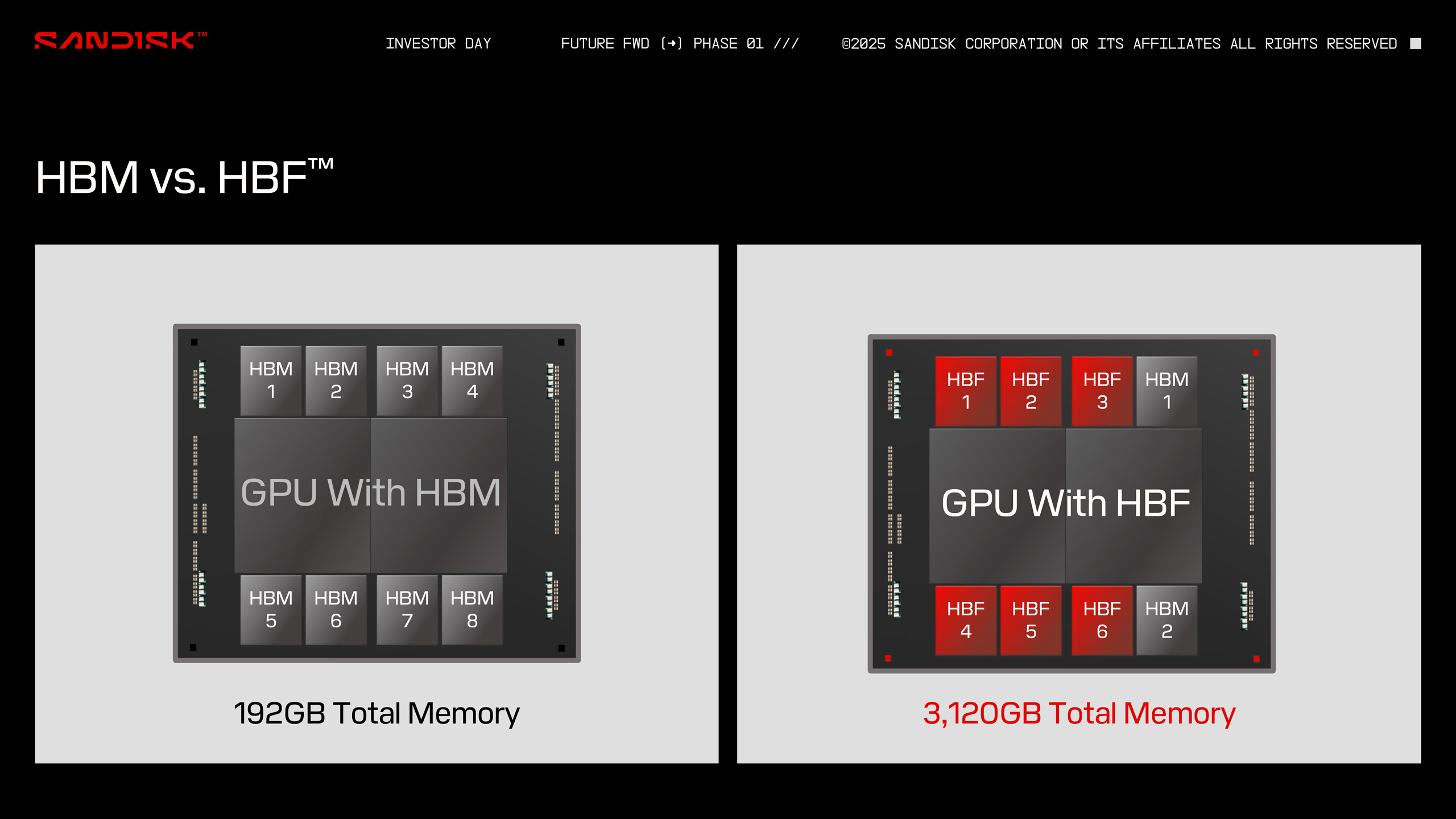
The only thing we know from a SanDisk-provided example is that eight HBF stacks feature 4 TB of NAND memory, so each stack can store 512 GB (21x more than one 8-Hi HBM3E stack that has a capacity of 24 GB). A 16-Hi 512 GB HBF stack means that each HBF core die is a 256 Gb 3D NAND device with some complex logic enabling die-level parallelism. Funneling hundreds of gigabytes of data per second from 16 3D NAND ICs is still quite a big deal, and we can only wonder how SanDisk can achieve that.
What we are sure about is that HBF will never match DRAM in per-bit latency, which is why SanDisk stresses that HBF products are aimed at read-intensive, high-throughput applications, such as big AI inference datasets. For many AI inference tasks, the critical factor is high throughput at a feasible cost rather than the ultra-low latency that HBM (or other types of DRAM) provides. So, while HBF may not replace HBM any time soon, it might occupy a spot on the market that requires high-capacity, high-bandwidth, NAND-like cost but not ultra-low latency. To simplify the transition from HBM, HBF has the same electrical interface with some protocol changes, though HBF is not drop-in compatible with HBM.
" We have tried to make it as close as possible mechanically and electrically to the HBM, but there are going to be minor protocol changes required that need to be enabled at the host devices," said Ilkbahar.
SanDisk didn't touch on write endurance. NAND has a finite lifespan that can only tolerate a certain number of writes. While SLC and pSLC technologies offer higher endurance than the TLC and QLC NAND used in consumer SSDs, this comes at the expense of capacity and adds cost. NAND is also typically written to at block granularity, whereas memory is bit-addressable. That's another key challenge.
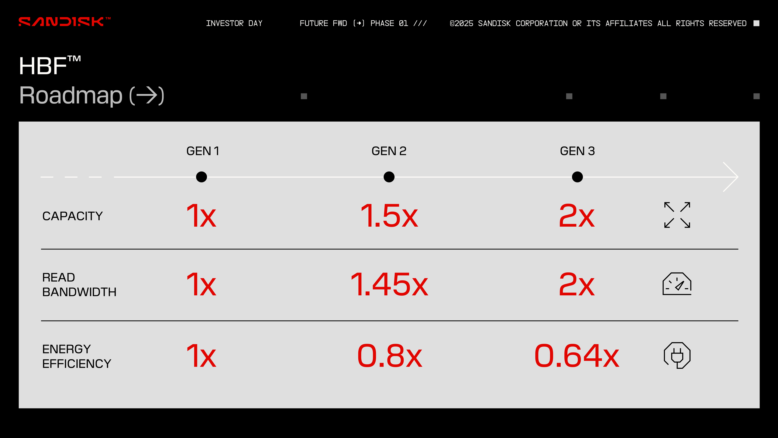
SanDisk has a vision of how its HBF will evolve over three generations. Nonetheless, for now, SanDisk's HBF is largely a work in progress. SanDisk wants HBF to become an open standard with an open ecosystem, so it is forming a technical advisory board consisting of 'industry luminaries and partners.