Samsung is set to tape out its first HBM4 memory devices later this year with sampling set to begin in early 2025, reports nN Elec citing industry sources. The company is projected to use its latest-generation 10nm-class DRAM fabrication process to make HBM4 DRAM devices as well as its 4nm-class logic technology to produce HBM4 base dies, the report says.
After Samsung tapes out its first HBM4 memory devices and base dies, its memory and logic fabs will have to produce and assemble them, which will take a couple of months or more. After that, Samsung will test these HBM4 stacks internally and then will start sampling them with its major customers, which in the case of HBM4 means leading producers of AI and HPC processors. Samsung declined to comment on its HBM4 timeline. Samsung may start mass production of HBM4 by late 2025, though it remains to be seen when actual products using the technology emerge.
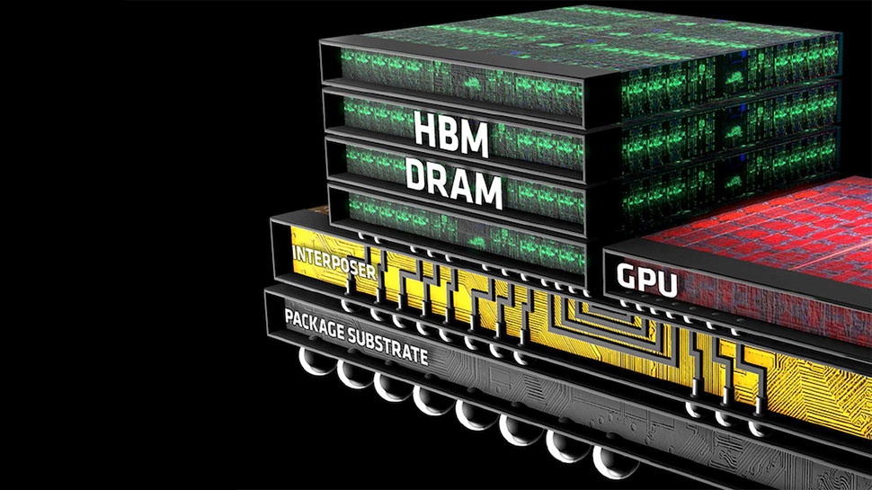
The company is set to use its latest-generation 10nm-class DRAM fabrication process (10c nm, 12nm) to make HBM4 memory layers as well as its 4nm-class logic production node to make HBM4 base dies with a 2048-bit interface, the report claims. Base dies made on such a fine manufacturing technology can be installed directly on processors using Samsung's own SAINT-D or similar techniques.
The upcoming HBM4 standard will define 24 Gb and 32 Gb layers as well as 4-high, 8-high, 12-high, and 16-high TSV stacks. It is hard to predict the configuration of Samsung's initial HBM4 modules, though the report says that the company would mass produce 12-High HBM4 stacks in the second half of next year. Speed bins of these modules will depend on multiple factors, though JEDEC's preliminarily settled speed bins reach up to 6.4 GT/s.
Samsung's arch-rival SK Hynix is also set to mass produce HBM4 in the second half of the year, the report says, though it does not disclose when SK Hynix's HBM4 sampling is set to start. While SK Hynix initially leaned towards using 1b DRAM technology for HBM4 memory layers, Samsung's decision to go with 1c production has prompted reconsideration, according to The Elec.
SK hynix will collaborate with TSMC to build base dies for its HBM4 memory modules. At the European Technology Symposium 2024, TSMC revealed plans to produce these base dies using its advanced 12FFC+ (12nm-class) and N5 (5nm-class) process technologies. TSMC's N5 logic technology will allow for denser logic integration and finer interconnection pitches to place memory directly on CPUs and GPUs. By contrast, base dies made with TSMC's 12FFC+ process will enable cost-effective base dies that use silicon interposers to connect memory to host processors.


.png?w=600)