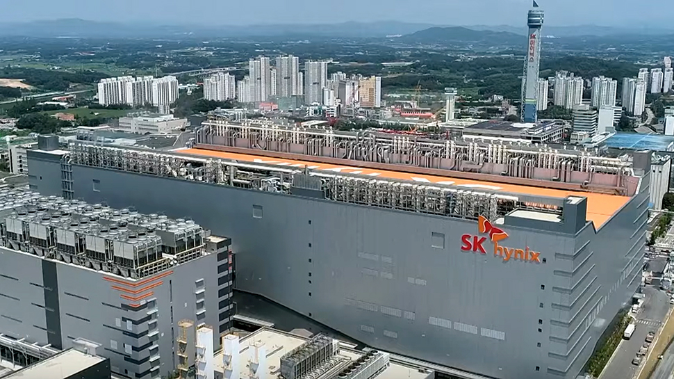
South Korean memory giant SK Hynix has been making a number of big announcements in recent months, including its plans to build the world's largest chip factory and the creation of a mobile storage chip that could make phones and laptops run faster.
The company has also begun collaborating with Taiwanese semiconductor foundry, TSMC, to develop and produce the next-generation of High Bandwidth Memory, known as HBM4, which will significantly boost HPC and AI performance, and could end up in Nvidia's purported H300 GPU.
At the recent 2024 IEEE 16th International Memory Workshop (IMW 2024) held in Seoul, South Korea, SK Hynix revealed more details about its plans for HBM4, which is expected to be widely available in 2026 (more on that in a second). As the largest maker of HBM, the company naturally had a lot to say on the topic.
Accelerating HBM development
The company’s development roadmap shows that HBM4 will have the same die density as HBM3E (24Gb), but with 16 layers instead of 12. It will also offer 1.65TB/s bandwidth, compared to HBM3E's 1.18TB/s. The capacity will be 48GB, up from 36GB, with a total IO/cube of 2048 pins, double that of its predecessor. SK Hynix claims that the power consumption of the chip will be reduced to around half.
According to PC Watch, "The keynote speech also touched on the next generation of the HBM4E module. Commercialization is planned for 2028. The maximum input/output bandwidth is likely to be over 2TB/s. Details such as storage capacity and DRAM die are unknown."
What's really interesting is that PC Watch also reports that at the end of the keynote, there was a slide stating that the company's production schedule is going to be accelerated, and that "commercialization of the 'HBM4' module will be brought forward to 2025 and the 'HBM4E' module to 2026."
If that is the case, it's likely that SK Hynix is responding to the threat from its archrival Samsung, which is developing its own HBM4 module which is expected to debut next year.


