Zelenograd Nanotechnology Center (ZNTC) and Planar have concluded developing Russia's first lithography system capable of supporting 350nm-class process technologies (0.35 micron). The development was assisted by Belarus-based Planar company. The machine has cleared official inspections and is undergoing integration trials in Zelenograd. Despite its symbolic significance, the system's design has been outdated by several decades, and whether ZNTC can produce these in volume is unclear.
A new tool
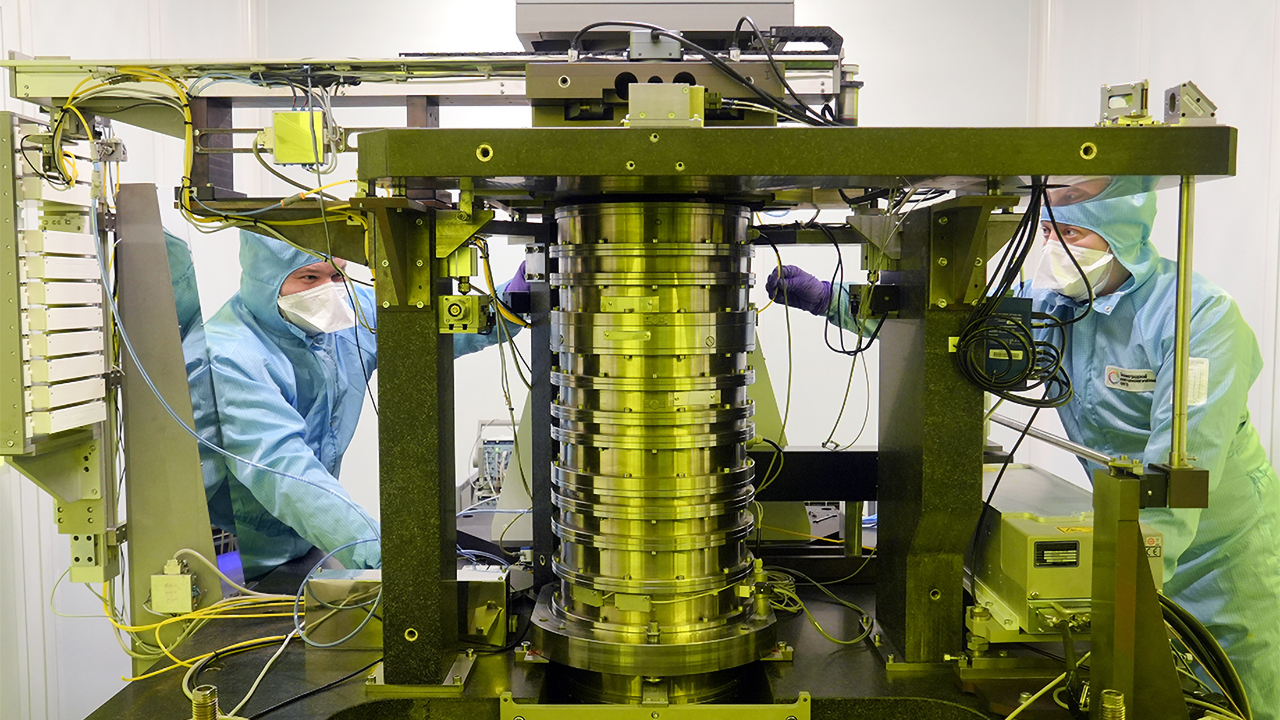
The ZNTC lithography tool — which was officially introduced a year ago — is a 200-mm litho machine based on a solid-state laser with an exposure field size of 22mm × 22mm (484 mm^2). ZNTC and Planar do not disclose critical technical details about the tool, including the wavelength of the laser it uses or the power that the laser can emit. However, it says it uses an energy-efficient 'solid-state' laser with a 'tighter' emission range and longer operational life.
The use of a solid-state light source seems to be an important detail that not only differentiates the tool from those designed by leading fab tool makers but could also give a hint about the company's plans going forward.
Considering that ZNTC makes rather vague announcements (perhaps to keep its progress and the progress of its partners under wraps), it makes sense to examine the so-called best-known production tools from ASML to put ZNTC's achievements into context.
ASML's lithography tools designed for 200-mm wafers used for process technologies ranging from 350nm down to 130nm traditionally utilized one of two main types of ultraviolet (UV) illumination sources, depending on the exact lithography model and process node requirements: mercury arc lamps, KrF (krypton fluoride), or ArF (argon fluoride) laser.
For process technologies of 350nm and less advanced, ASML's i-line steppers used mercury arc lamps with a wavelength of 365nm(405nm and 436nm were less common). For nodes of 250nm and more advanced, ASML used a KrF (krypton fluoride) laser with a 248nm wavelength. Starting from 130nm nodes, ASML's deep ultraviolet lithography systems have used ArF (argon fluoride) lasers with a 193nm wavelength.
A solid-state light source?
An avid reader would ask, "What is a solid-state laser in semiconductor production?" Solid-state lasers are widely used in semiconductor manufacturing, yet not for the primary lithographic exposure at advanced nodes. Instead, they are used in supporting roles, such as wafer inspection, defect analysis, marking, and micromachining processes, including wafer dicing or trimming components.
Solid-state lasers operating at around a 365nm wavelength (frequency-tripled Nd:YAG lasers) can also be employed for lithography at mature nodes (e.g., ≥250nm), as they are stable, efficient, and reliable. However, as noted above, ASML has used gas-based excimer lasers (KrF at 248nm, ArF at 193nm) or mercury lamps (365nm i-line) since the late 1990s.
This gets interesting as ZNTC said it is working on a lithography system capable of a 130nm-class process technology, though its development is expected to be finalized sometime in 2026.
Too late?
While a 350nm-class process technology is used for some devices, it is obsolete by today's standards. In the mid-1990s, Intel used this node for its Pentium MMX, Pentium Pro, and early Pentium II CPUs, while AMD produced its K6 processor using the same technology around 1997. Nowadays, advanced chips are made at 5nm-class process technologies or better.
Even Russian chipmakers like Angstrem and Mikron do not manufacture at 350 nm. Both companies operate at resolutions between 250 nm and 90 nm. As such, the new scanner does not match the existing production nodes of major Russian foundries, limiting its immediate commercial relevance to non-critical layers at domestic producers, which will continue to use ASML's PAS 5500-series lithography tools, which are smuggled into Russia.
Still, ZNTC's tool may find limited use in specific sectors. Some automotive and power management ICs are produced using mature processes. Military applications could also benefit from this kind of tool, as cutting-edge performance is not always a requirement for them.
Still, it appears that the new machine's primary aim is to serve as a base for developing more capable versions. ZNTC is currently working on a new model targeting 130nm-class process technologies. Completion is expected in 2026. This version is part of a longer-term roadmap set by the Russian government, which aims for domestic production at 90nm by the end of 2025, 28nm by 2027, and 14nm by 2030. ZNTC and its peers in Russia are well behind the plan.