Scientists have developed a new type of razor-thin crystal film semiconductor that enables electrons to move seven times faster than they do in traditional semiconductors — and it could have huge implications for electronic devices.
In a study published July 1 in the journal Materials Today Physics, physicists created an extremely thin film from a crystalline material called ternary tetradymite.
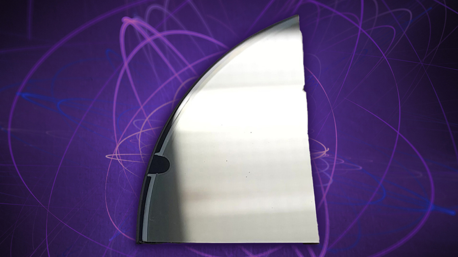
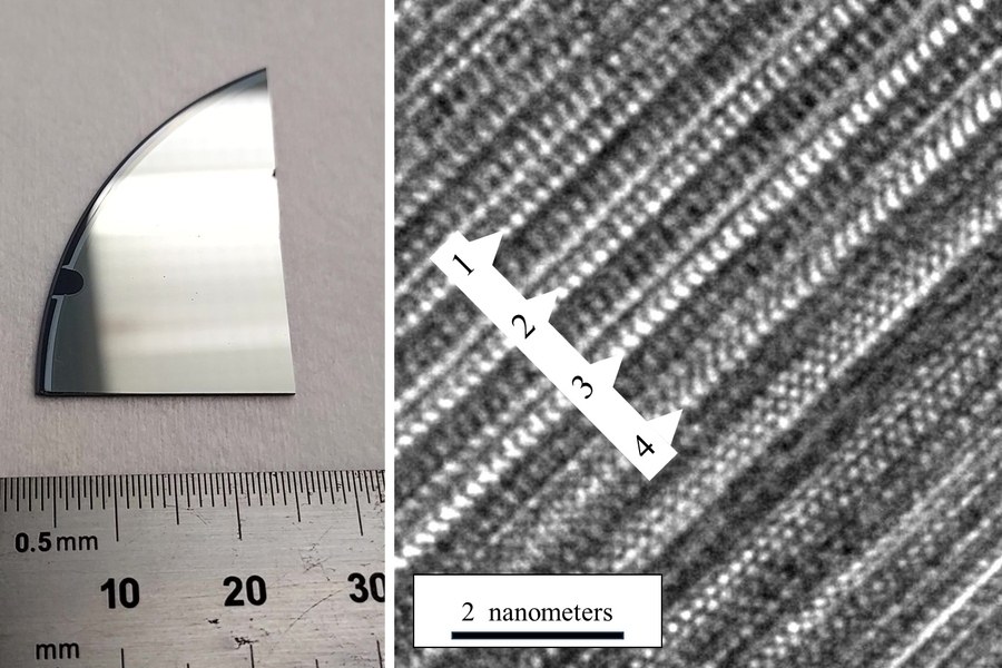
The film — measuring just 100 nanometers wide, or about one-thousandth of the thickness of a human hair — was created through a process called molecular beam epitaxy, which involves precisely controlling beams of molecules to build a material atom-by-atom. This process allows materials to be constructed with minimal flaws or defects, enabling greater electron mobility, a measure of how easily electrons move through a material under an electric field.
When the scientists applied an electric current to the film, they recorded electrons moving at record-breaking speeds of 10,000 centimeters squared per volt-second (cm^2/V-s). By comparison, electrons typically move at about 1,400 cm^2/V-s in standard silicon semiconductors, and considerably slower in traditional copper wiring.
Related: Charging future EVs could take seconds with new sodium-ion battery tech
This sky-high electron mobility translates to better conductivity. That, in turn, paves the way for more efficient and powerful electronic devices that emit less heat and waste less energy.
The researchers likened the film's properties to "a highway without traffic," saying that such materials "will be essential for more efficient and sustainable electronic devices that can do more work with less power." Potential applications include wearable thermoelectric devices that convert waste heat into electricity and "spintronic" devices, which use electron spin instead of charge to process information, the scientists said.
"Before, what people had achieved in terms of electron mobility in these systems was like traffic on a road under construction — you’re backed up, you can’t drive, it’s dusty, and it’s a mess," Jagadeesh Moodera, a physicist at MIT, said in a statement. "In this newly optimized material, it’s like driving on the Mass Pike with no traffic."
The scientists measured electron mobility in the material by placing the crystalline film in an extremely cold environment under a magnetic field. They then passed electrical current through it and measured quantum oscillations, which occur when electrical resistance fluctuates in response to a magnetic field.
Even tiny defects in the material can affect electronic mobility by obstructing the movement of electrons. As such, the scientists hope that refining the process for creating the film will produce even better results.
"This is showing it’s possible to go a giant step further, when properly controlling these complex systems," Moodera said. "This tells us we’re in the right direction, and we have the right system to proceed further, to keep perfecting this material down to even much thinner films and proximity coupling for use in future spintronics and wearable thermoelectric devices."