On Friday, the JEDEC Association published preliminary specifications for the 4th Generation high-bandwidth memory (HBM4) as it is getting closer to completing the HBM4 DRAM standard. As reported, the new spec supports a 2048-bit interface per stack amid a lower data transfer rate than HBM3E. In addition, HBM4 supports a broader range of memory layers to make the new memory better address different types of applications.
The new HBM4 standard will specify 24 Gb and 32 Gb layers and offer configurations for 4-high, 8-high, 12-high, and 16-high TSV stacks. The committee has initially agreed on speed bins up to 6.4 GT/s, with ongoing discussions about achieving an even higher data transfer rate.
A 16-Hi stack based on 32 Gb layers will offer a capacity of 64 GB, which means that a processor with four memory modules can support 256 GB of memory with a peak bandwidth of 6.56 TB/s using an 8,192-bit interface.
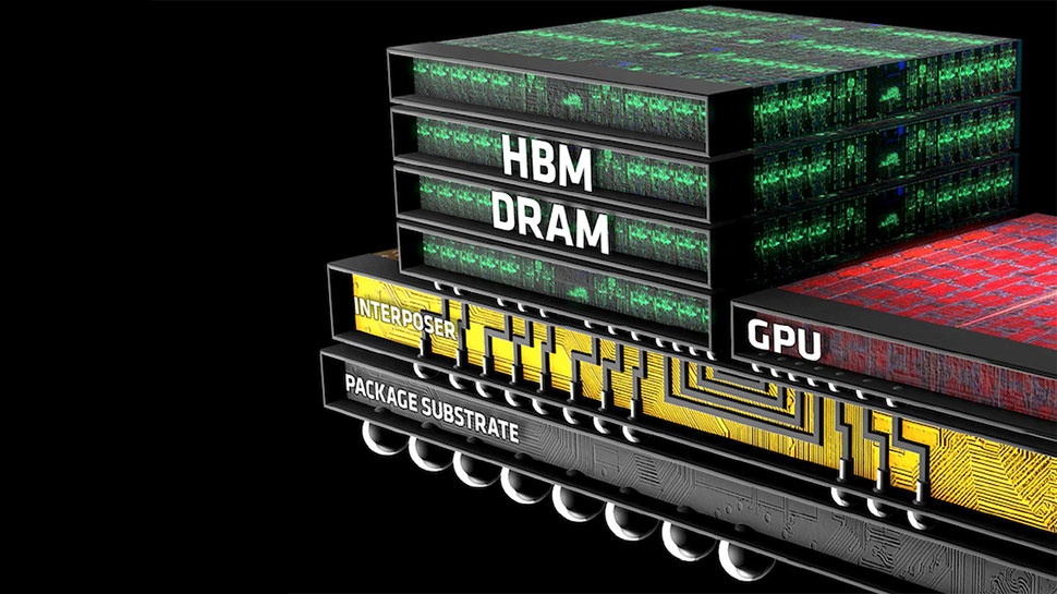
Although HBM4 will feature a doubled channel count per stack compared to HBM3 and a larger physical footprint to ensure compatibility, a single controller can work with HBM3 and HBM4. However, different interposers will be needed to accommodate the various footprints. What is noteworthy is that JEDEC did not say anything about integrating HBM4 memory directly on processors, and that is perhaps the most intriguing part about the new type of memory.
Earlier this year, SK hynix and TSMC announced a collaboration to develop HBM4 base dies. Later on, at the European Technology Symposium 2024, TSMC confirmed it would use its 12FFC+ (12nm-class) and N5 (5nm-class) process technologies to manufacture these dies.
TSMC's N5 process allows for more integrated logic and features, with interconnection pitches from 9 to 6 microns, which is crucial for on-die integration. The 12FFC+ process, derived from TSMC's 16nm FinFET technology, will enable the production of cost-effective base dies that connect memory to host processors using silicon interposers.
HBM4 is primarily designed to meet the demands of generative AI and high-performance computing, which require handling large datasets and performing complex calculations efficiently. Therefore, we are hardly going to see HBM4 on client applications, such as graphics cards.