A leaker from the Chipell forums (via HXL) published images of Nvidia-designed PCBs (printed circuit boards) that were used to bring up the new Blackwell RTX 50-series GPUs while the company was developing its latest graphics cards. The boards feature debugging interfaces alongside overwhelming power delivery circuitry, with the latter allowing designers to better understand how particular GPUs work and respond to various factors.
🥲nvidia engineering samplesAD102: 4x 16pinGB202: 4x 16pinproduction card4090:1x 16pin5090:1x 16pinhttps://t.co/c4RAWWfO4u pic.twitter.com/ReybcTsdeUFebruary 11, 2025
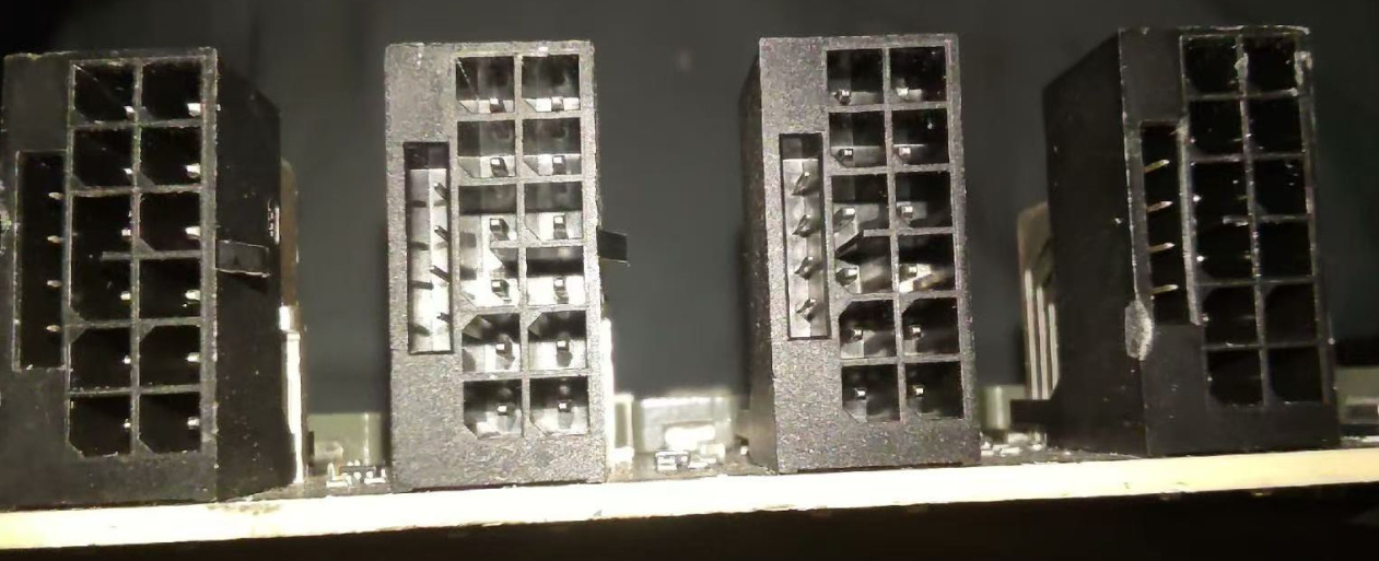
As an example of this, development/bring up boards for Nvidia's GeForce RTX 4090 (AD102) and RTX 5090 (GB202) — according to blogger Panzerlized — feature four 16-pin 12VHPWR and 12V-2x6 power connectors, respectively. By contrast, development cards for the GeForce RTX 3090 (GA102) and RTX 3080 (GA104) featured four or three 8-pin power connectors. So it's not just the latest GPUs, as older-generation products also featured an 'excessive' number of power connectors.
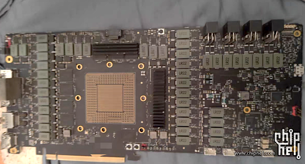
The higher number of power connectors on development/bring-up boards is not surprising or indicative of any underlying problems. Engineers tend to power up such graphics cards in stages, including core voltages, uncore voltages, memory voltages, I/O rails, and so on. This is done to verify that all power the rails initialize correctly, and that no short-circuit or out-of-spec behavior occurs.
The cards also feature debugging interfaces, test points, and instrumentation headers to allow for in-depth measurement and monitoring. All these are present on the cards pictured. Finally, there are plenty of jumpers on the PCBs to reconfigure various things.
As an added bonus, these boards can deliver an excessive amount of power to the GPUs. This can help Nvidia and its partners determine the exact capabilities and limits of the processors, as well as testing their performance under various conditions. For example, a prototype GeForce RTX 4090 had as many as 45 power phases along with four 12VHPWR power connectors. That's enough to deliver up to 2400 watts to the card, which far exceeds the amount of power required by the end product. (And we suspect Nvidia never actually tried to feed 2400W into a prototype.)
Some extreme overclockers would probably be excited to acquire such a graphics cards. The excessive power delivery setup could help with liquid nitrogen cooling, as one possibility. However, these development/bring up boards usually come with older BIOS versions that only work with select GPUs, and due to their early nature there's a good chance that they won't fully work or behave as expected. Getting drivers that support such cards could also be difficult.
Regardless, it's interesting to see the development boards used by Nvidia and its graphics cards partners. Designing, prototyping, testing, debugging, and finalizing modern computer components can be a very complex process, and even with all the work that goes into the launch of a new GPU, issues can crop up once cards are in the hands of thousands of gamers with a wide variety of hardware configurations.