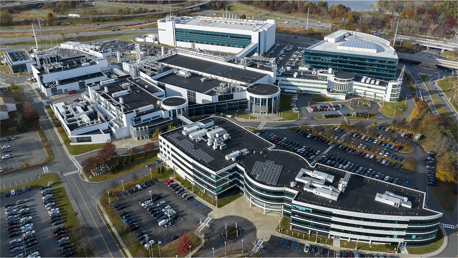
The Biden White House announced that it's investing $825 million in Albany, New York, to build the flagship facility of the National Semiconductor Technology Center (NSTC). The NSTC is America’s premier research and development center that aims to bolster innovations in semiconductor technology, develop a skilled workforce to support these new developments and collaborate with the private sector and academe. The U.S. Department of Commerce says that the Albany, New York site will focus on extreme ultraviolet (EUV) lithography — technology for manufacturing the most advanced nodes required for the next generation of chips and processors.
NSTC’s first facility, to be called CHIPS for America Extreme Ultraviolet (EUV) Accelerator, will take shape within the Albany NanoTech Complex—a high-tech site boasting over 1.65 million square feet of space—operated by the non-profit New York Center for Research, Economic Advancement, Technology, Engineering, and Science (NY CREATES). As the name suggests, this development is funded under the CHIPS and Science Act, which is America’s most significant investment in its semiconductor industry over the past 28 years combined.
“With this first proposed flagship facility, CHIPS for America is providing access to cutting-edge research and tools to the NSTC and its launch represents a key milestone in ensuring the United States remains a global leader in innovation and semiconductor research and development,” said Secretary of Commerce Gina Raimondo.
Raimondo states that “the research and development component of the CHIPS and Science Act is fundamental to our long-term national security and ensuring the U.S. remains the most technologically competitive place on earth. Thanks to President Biden and Vice President Harris, we are not just producing the world’s most advanced semiconductors; we are building a resilient ecosystem that will power everything from smartphones to advanced AI, safeguarding U.S. national security and keeping America competitive for decades to come.”
EUV technology enables companies to push the boundaries of Moore’s Law, which states that the number of transistors in an integrated chip doubles every year. As the latest processors have already hit over 100 billion transistors on a single chip, we need further advancements in EUV lithography to allow us to pack in even more transistors in the same amount of space.
Currently, Netherlands-based ASML is the only company in the world that produces High-NA EUV machines needed to make the latest generation of chips. As the U.S. aims to consolidate its semiconductor supply chain, it needs homegrown technologies, materials, and companies that will allow it to safeguard its chip sources — from mining the rare earth metals required to make the high-purity silicon needed to make semiconductor wafers to the machines needed to manufacture the most advanced processors. While it will take years, perhaps even decades, to achieve this, establishing this research facility is a step in the right direction.


