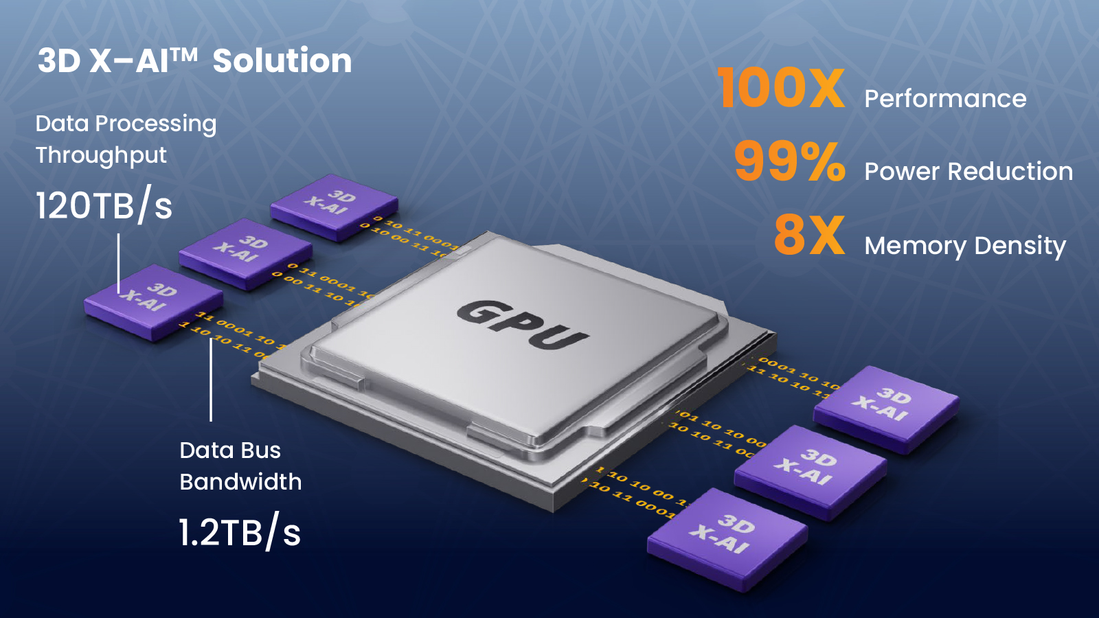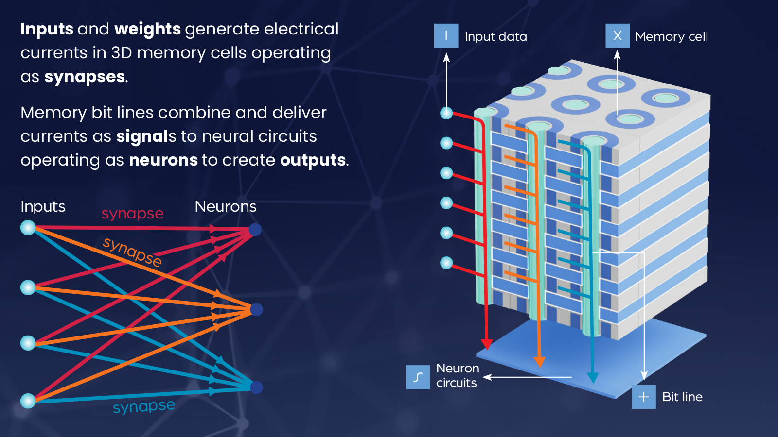
NEO Semiconductor, focusing on 3D NAND flash memory and 3D DRAM, announced 3D X-AI chip technology to replace the HBMs currently used in AI GPU accelerators. This 3D DRAM has built-in AI processing that lets it process and generate outputs that do not require mathematical calculations. It reduces the data bus bottleneck problems when massive amounts of data are transferred between the memory and processor, increasing AI performance and efficiency.
The 3D X-AI chip has a neuron circuit layer at its base, which processes the data stored in the 300 memory layers on the same die. According to NEO Semiconductor, this 3D memory offers a 100-fold performance improvement due to its 8,000 neutron circuits that do AI processing in memory. It also has eight times more memory density than current HBMs and, more importantly, offers a 99% power reduction by reducing the amount of data that needs to be processed in the power-hungry GPUs.
"Current AI Chips waste significant amounts of performance and power due to architectural and technological inefficiencies," says NEO Semiconductor Founder & CEO Andy Hsu.
Hu commented, "The current AI Chip architecture stores data in HBM and relies on a GPU to perform all calculations. This separated data storage and data processing architecture makes the data bus an unavoidable performance bottleneck. Transferring huge amounts of data through the data bus causes limited performance and very high power consumption. 3D X-AI can perform AI processing in each HBM chip. This can drastically reduce the data transferred between HBM and GPU to improve performance and reduce power consumption dramatically."

The company says that X-AI has a capacity of 128GB and can support 10 TB/s of AI processing per die. Stacking twelve dies together in a single HBM packaging could achieve a storage capacity of more than 1.5TB and 120 TB/s of processing throughput.
AI development is pushing the edge of computing, with many companies researching technology that will increase processing speeds and communication throughput as well. As we get faster and more efficient semiconductors, the bus that transfers data between components becomes the bottleneck. So, technologies like this will allow all components to go faster together.
For example, several companies, including Intel, Kioxia, and TSMC, have been working on optical technology to allow for faster communications within the motherboard. But by transferring some of the AI processing from the GPU to the HBM, NEO Semiconductor could help reduce its workload, thus making it far more efficient than the current power-hungry AI accelerators.


