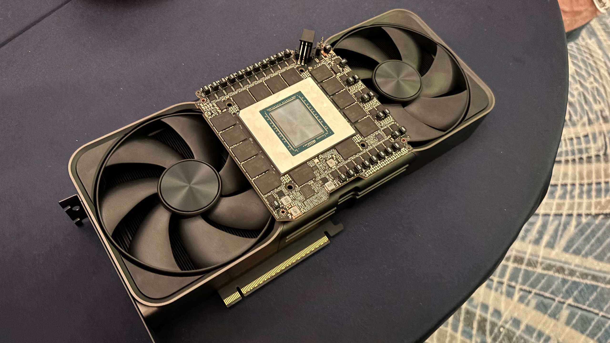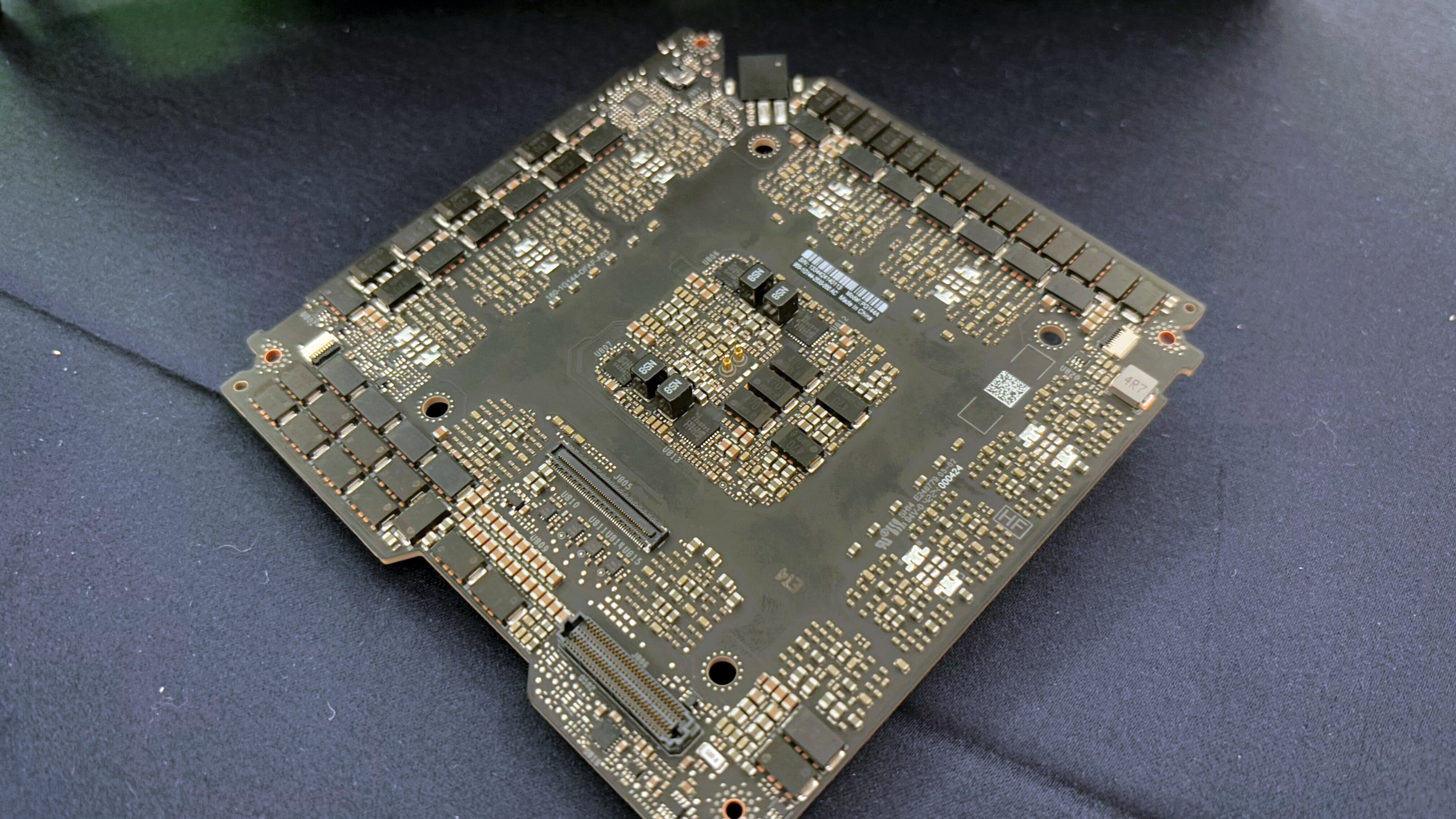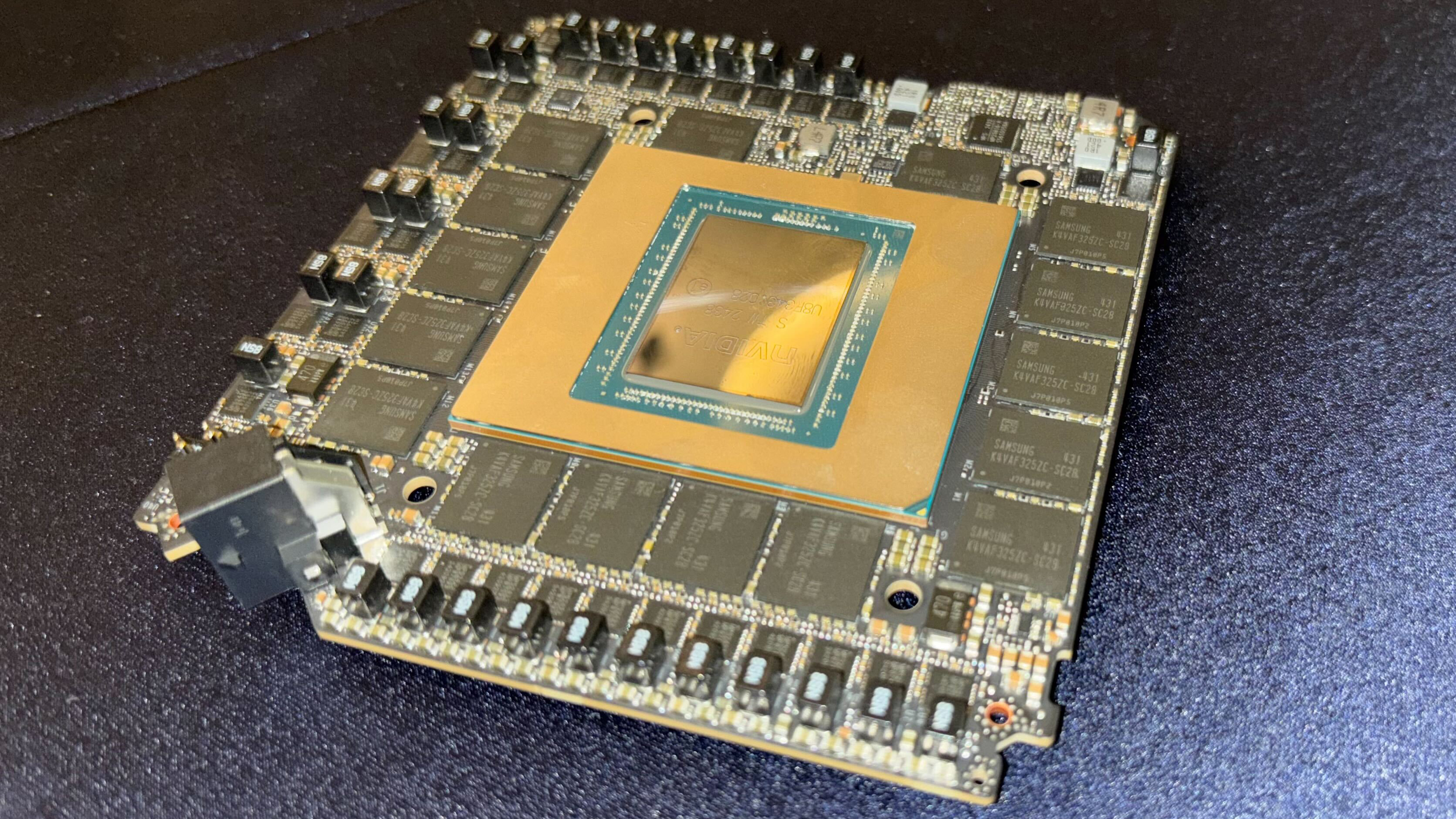
Nvidia's GeForce RTX 5090 Founders Edition graphics board — which promises to be the best graphics card around — uses an unorthodox three-piece printed circuit board (PCB), and the high-density board, which carries the graphics processor, memory, and power supply circuitry, poses many mysteries. Now that we have pictured both the front and back sides of the main GeForce RTX 5090 FE PCB, we can reveal at least some of them.
We already know quite a lot about the front side of the board — which carries a GB202 GPU, 32GB of GDDR7 memory from Samsung (using 16 packages marked as K4VAF3257C-SC28), and a 30-phase voltage regulation module — so check out our coverage from earlier this week. But we have not seen the backside until today.

The backside has four more power delivery phases, which means that Nvidia's GeForce RTX 5090 Founders Edition graphics card uses a rather extraordinary 34-phase VRM. Also, there is a relatively large high‐density board‐to‐board (mezzanine) connector (marked as J806) often used in compact electronics to mate two circuit boards together, and a smaller mezzanine connector marked as J805. In addition, there are two ZIF connectors for fans.

We can only wonder what exactly the J805 and J806 connectors are used for, but common sense tells us they connect the PCBs with a set of display outputs and a PCIe x16 grid. We are unsure which connector transmits standard DisplayPort and HDMI signals or is part of a proprietary high-speed interface connecting to an ASIC, enabling standard DP and HDMI outputs.
Usually, a small PCB — such as the one that carries the GB202 GPU and its memory — allows much more space for airflow and cooling. However, as the main board will need two additional boards to be attached, it remains to be seen how this affects internal airflow. This does not make this particular PCB less impressive, as a tiny board that can supply 575W (and potentially more) of power to the GPU and its memory is certainly an achievement, particularly in the consumer electronics market.
Finally, there are two spring‐loaded contacts (POGO pins) below the GPU that are often used as test or programming contacts, which indicates that we may not be dealing with a final version of the PCB. This is not surprising, as the GPU was made during the 38th week of 2024, which is mid-September.


