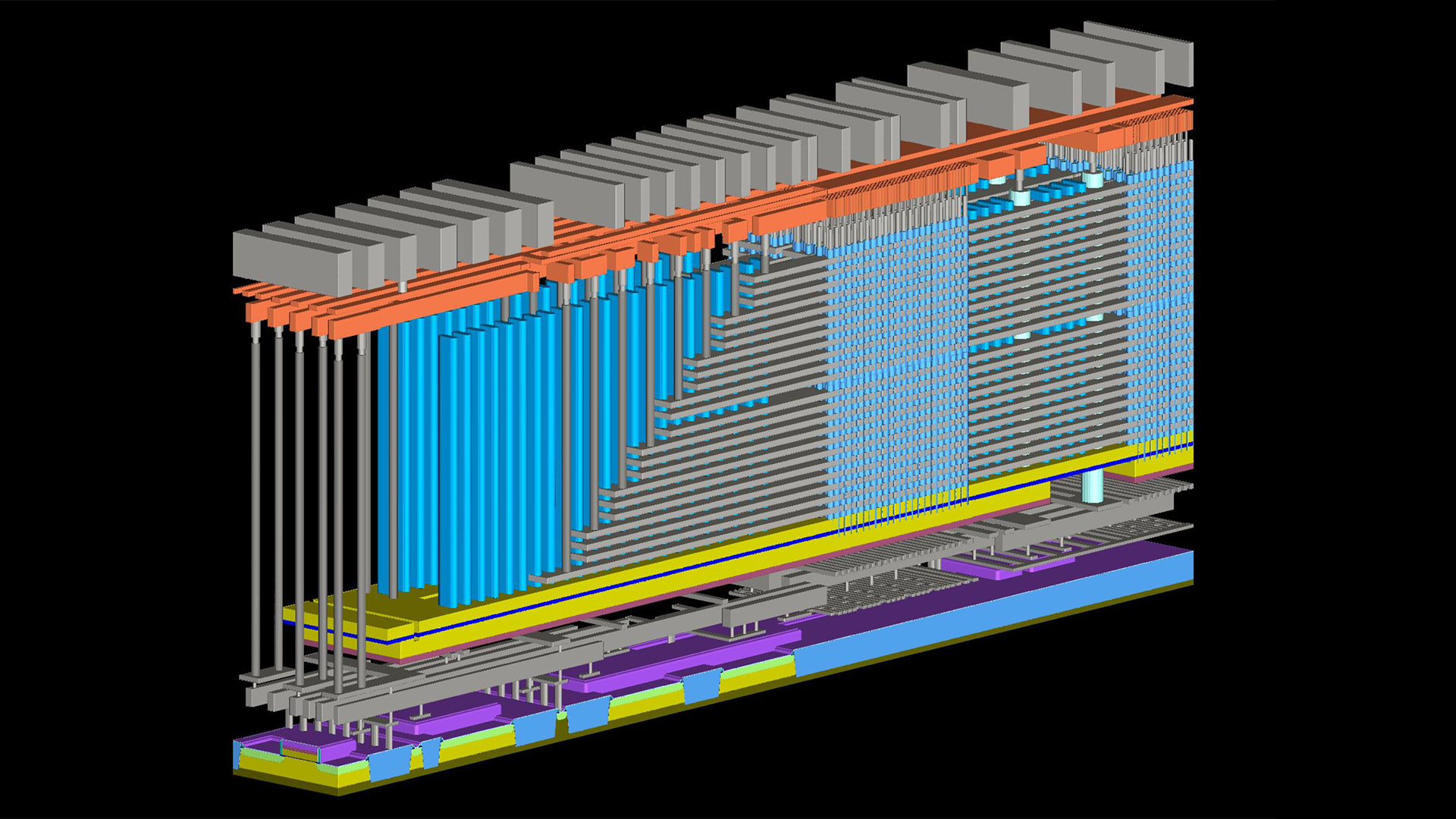
Kioxia and its research and manufacturing partner Western Digital plan to reveal their innovations that will enable higher-capacity and higher-performance 3D NAND memory devices at the upcoming 2023 Symposium on VLSI Technology and Circuits. Engineers from the two companies are looking to enable 8-plane 3D NAND devices as well as 3D NAND ICs with over 300 word-lines, reports eeNewsEurope.
Eight-Plane 3D NAND: Up to 205 MB/s
As 3D NAND devices increase the number of word-lines, shrink dimensions of NAND cells, and amplify the capacity of memory ICs, it becomes crucial to increase their read/write performance. Actual devices like the best SSDs, laptops, and smartphones tend to use fewer chips for a given capacity, but end users expect their new devices to be faster than their old ones.
One of the ways to improve performance of a 3D NAND IC is to increase the number of planes and enhance its internal parallelism. Kioxia will present a paper (C2-1) covering an eight-plane 1Tb 3D TLC NAND device with over 210 active layers and a 3.2 GT/s interface. The IC closely resembles Kioxia's/Western Digital's 218-layer 1Tb 3D TLC NAND device with a 17Gb/mm^2 density and a 3.2 GT/s I/O bus introduced in late March, but this one features eight planes instead of four and is said to offer 205 MB/s program throughput as well as a read latency of 40 μs. That latter spec is significantly better than the 56 μs offered by Kioxia's 128-layer 3D NAND.
The new paper reveals that Kioxia's 1Tb 3D TLC NAND device achieved its 3.2 GT/s interface speed by reducing the data query area in the X direction to 41%, allowing faster data transfer between memory and host. However, this new design can lead to wiring congestion, which Kioxia mitigated by introducing hybrid row address decoders (X-DEC). X-DECs help manage increased wiring density effectively, minimizing the degradation in read latency that could result from congestion.
Kioxia also implemented a one-pulse-two-strobe technique that allows for two memory cells to be sensed within a single pulse, reducing overall sensing time by 18% and increasing program throughput to 205 MB/s. The device's novel eight-plane architecture, one-pulse-two-strobe method, and 3.2 GT/s I/O allow for a read latency of 40 μs and a program throughput of 205 MB/s.
It's likely that the 1Tb 3D TLC NAND device already implements hybrid row address decoders and the one-pulse-two-strobe technique for its speedy interface, and these technologies will likely be widely used in the future. However, implementing an eight-plane architecture increases the complexity of both the 3D NAND IC and supporting memory controller, leading to higher development and manufacturing costs as well as longer time-to-market. Additionally, if the host controller cannot properly manage an eight-plane device, the actual performance of the IC may decrease.
>300-Layer 3D NAND
Besides investigating eight-plane 3D NAND IC device structures, Kioxia and Western Digital are also collaborating to develop 3D NAND devices with over 300 active word layers, which would enhance vertical channel length and boost the channel's crystalline quality.
To achieve this, the companies plan to employ Metal Induced Lateral Crystallization (MILC) techniques, as stated in the T7-1 paper. By utilizing MILC, developers were able to create single-crystallized 14-micron-long 'macaroni-like' silicon (Si) channels inside vertical memory holes, although for a 112-layer prototype device.
This experimental 3D NAND IC is also reported to leverage a cutting-edge nickel gettering method for eliminating impurities and flaws from the silicon material, thus enhancing cell array performance. As a result, read noise is reduced by a minimum of 40%, and channel conductance is increased tenfold, all without sacrificing cell reliability.
>400-Layer 3D NAND
Currently, techniques like string stacking allow for the construction of 3D NAND with hundreds of active layers, but they are time-intensive. As a result, device manufacturers and wafer fab equipment producers are developing methods to increase the layer count by etching longer (deeper) vertical channels.
Tokyo Electron, an etching tools manufacturer, is set to present a paper (T3-2) detailing a method for rapidly drilling more than 10-micron (10 μm) vertical channels for 400-layer 3D NAND nodes without excessive energy consumption or the use of toxic substances.
According to Tokyo Electron, its High-Aspect-Ratio (HAR) dielectric etching technology employs a cryogenic wafer stage and new gas chemistry to create 10-micron-high channels with an "excellent" etching profile in just 33 minutes and with an 84% reduced carbon footprint.


