Professor Tsumoru Shintake of the Okinawa Institute of Science and Technology (OIST) has proposed an all-new and greatly simplified EUV lithography tool that is cheaper than those developed and made by ASML. If the device hits mass production, it could reshape the chipmaking equipment industry, if not the whole semiconductor industry.
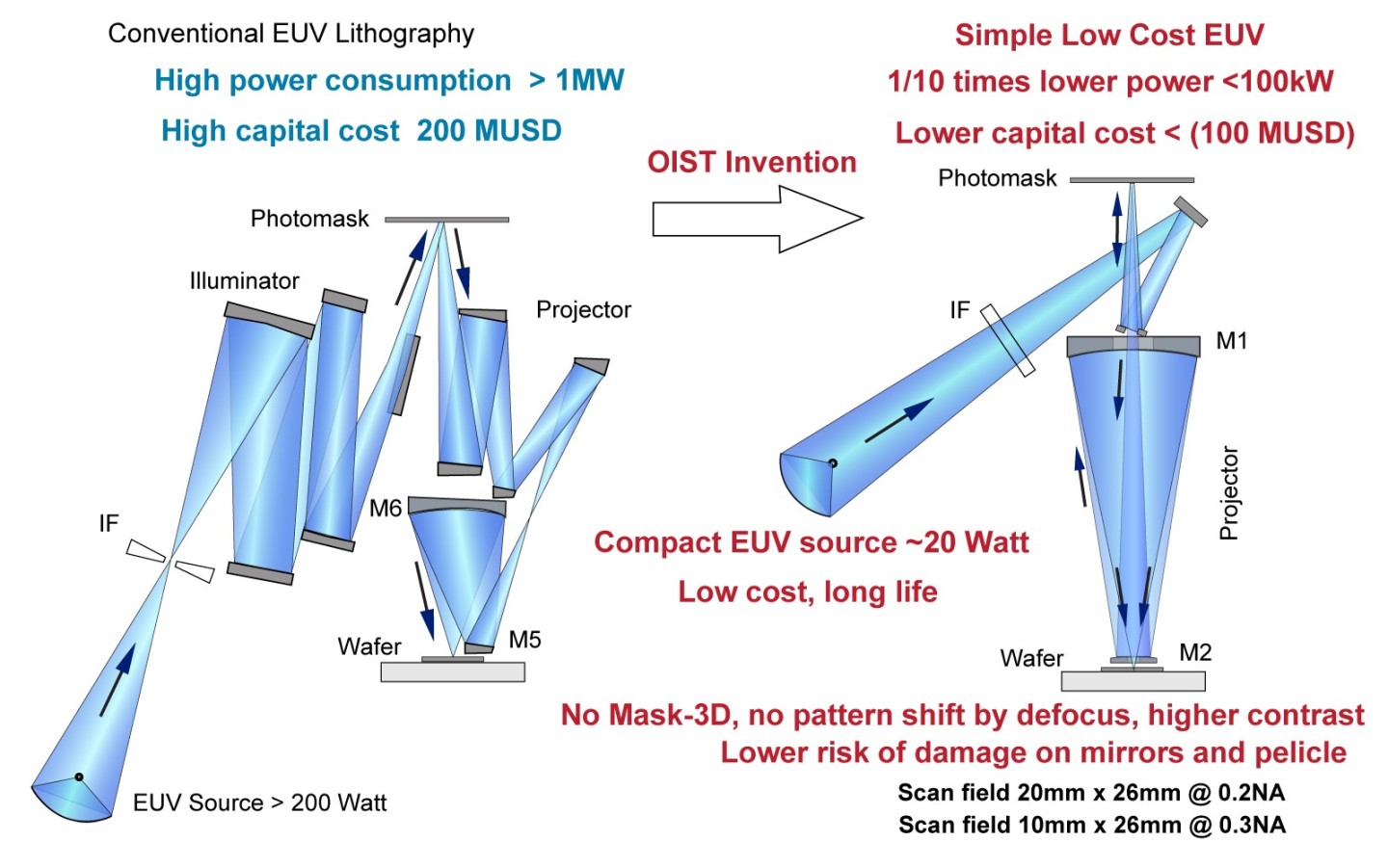
The new system uses only two mirrors in its optical projection setup, a significant departure from the conventional six-mirror configuration. The challenge of such an optical system is that it involves aligning these mirrors in a straight line, which ensures that the system maintains high optical performance without the usual distortions associated with EUV light. The new optical path allows more than 10% of the initial EUV energy to reach the wafer, compared to about 1% in standard setups, an improvement which is a major breakthrough.

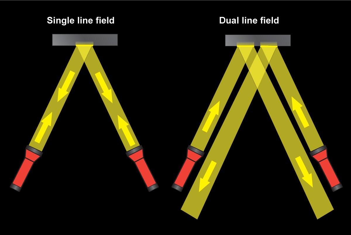
Professor Shintake's team solved two major challenges in EUV lithography: preventing optical aberrations and ensuring efficient light transfer. OIST's 'dual-line field' method illuminates the photomask without interfering with the optical path, which minimizes distortions and enhances image precision on the silicon wafer.
One of the key advantages of this minimalist design is that it enhances reliability and reduces maintenance complexities. Another advantage of this EUV lithography tool design is a drastic reduction of its power consumption. Thanks to the optimized optical path, the system operates with an EUV light source of just 20W, leading to a total power consumption of less than 100kW. In contrast, traditional EUV lithography systems often require over 1MW of power. Because of lower power consumption, the new litho system does not require a sophisticated and expensive cooling system.

The performance of this new system has been rigorously verified using optical simulation software, confirming its capability for producing advanced semiconductors. The technology's potential has led to a patent filing by OIST, indicating readiness for commercial deployment.
OIST is committed to advancing its EUV tool design further, aiming to bring it to practical application. The institute sees this innovation as a vital step toward solving global challenges, such as the costs of chip production and power consumption of semiconductor fabs, which affect the environment.
The economic implications of this invention are promising. The global EUV lithography market is expected to grow from $8.9 billion in 2024 to $17.4 billion by 2030. With this simplified design of EUV tools, the industry could adopt more EUV systems in the coming years. However, it is unclear how close OIST is to commercialization of its tool.


