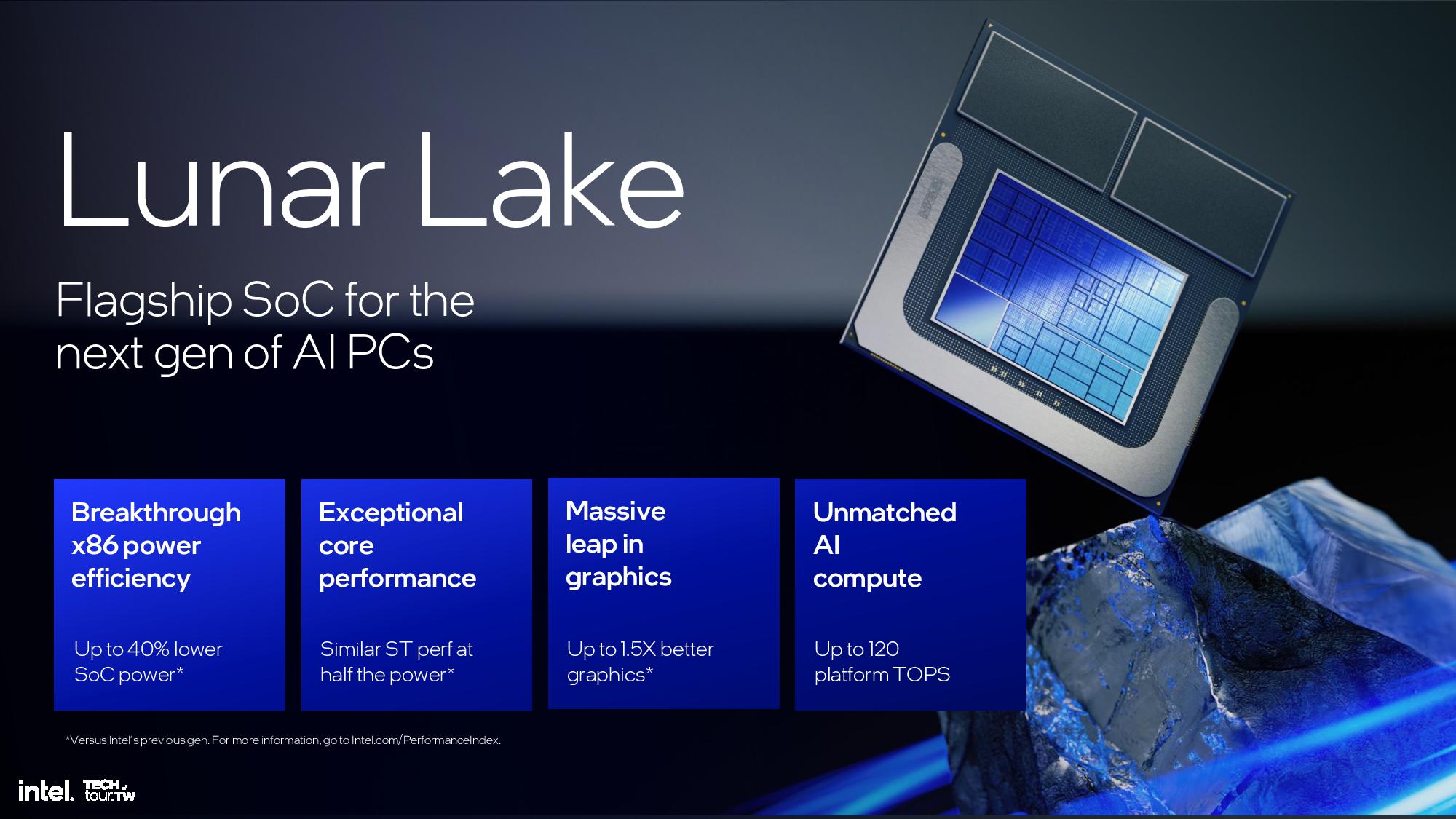
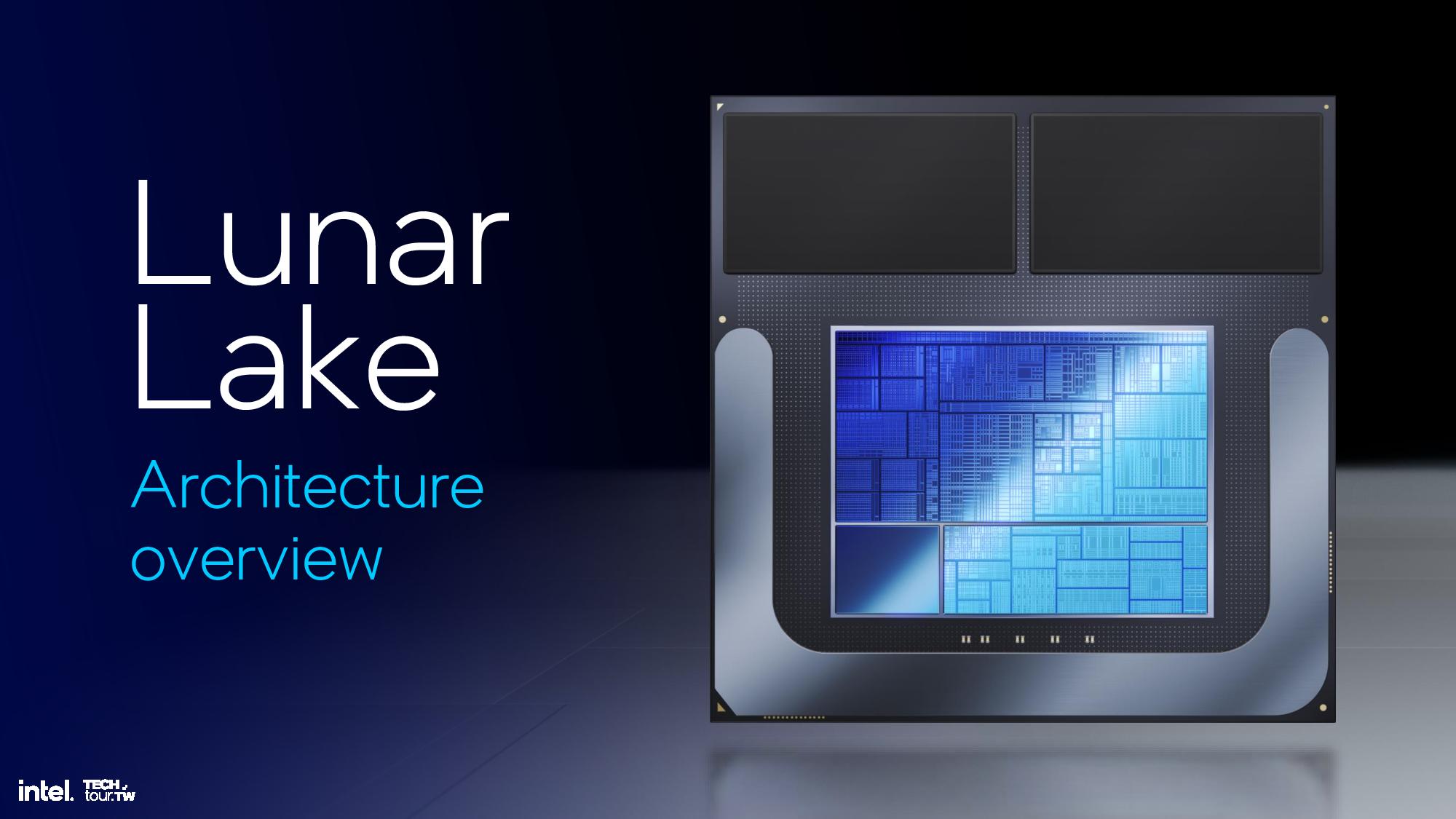
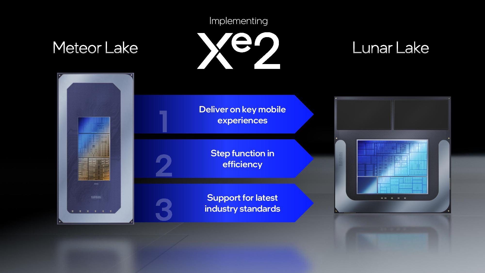
Intel pulled the covers back on its Lunar Lake architecture during its Intel Tech Tour 2024, delivering deep dive architectural details in Taipei, Taiwan in advance of the company’s Computex 2024 keynote as its newest chips race to a Q3 launch. Intel’s Lunar Lake will have significant improvements in every facet of its design. Lunar Lake will primarily target mobile designs, powering some of the best laptops, though many of the fundamental changes will likely carry over to Arrow Lake and will be in some of the best CPUs for gaming.
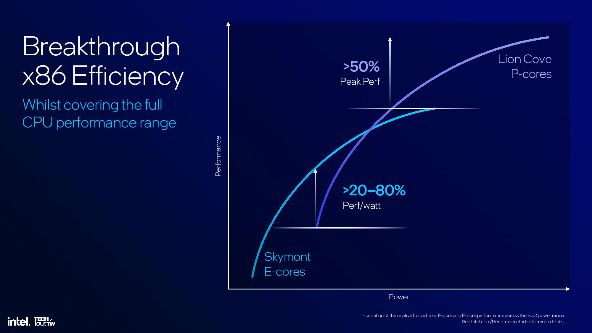
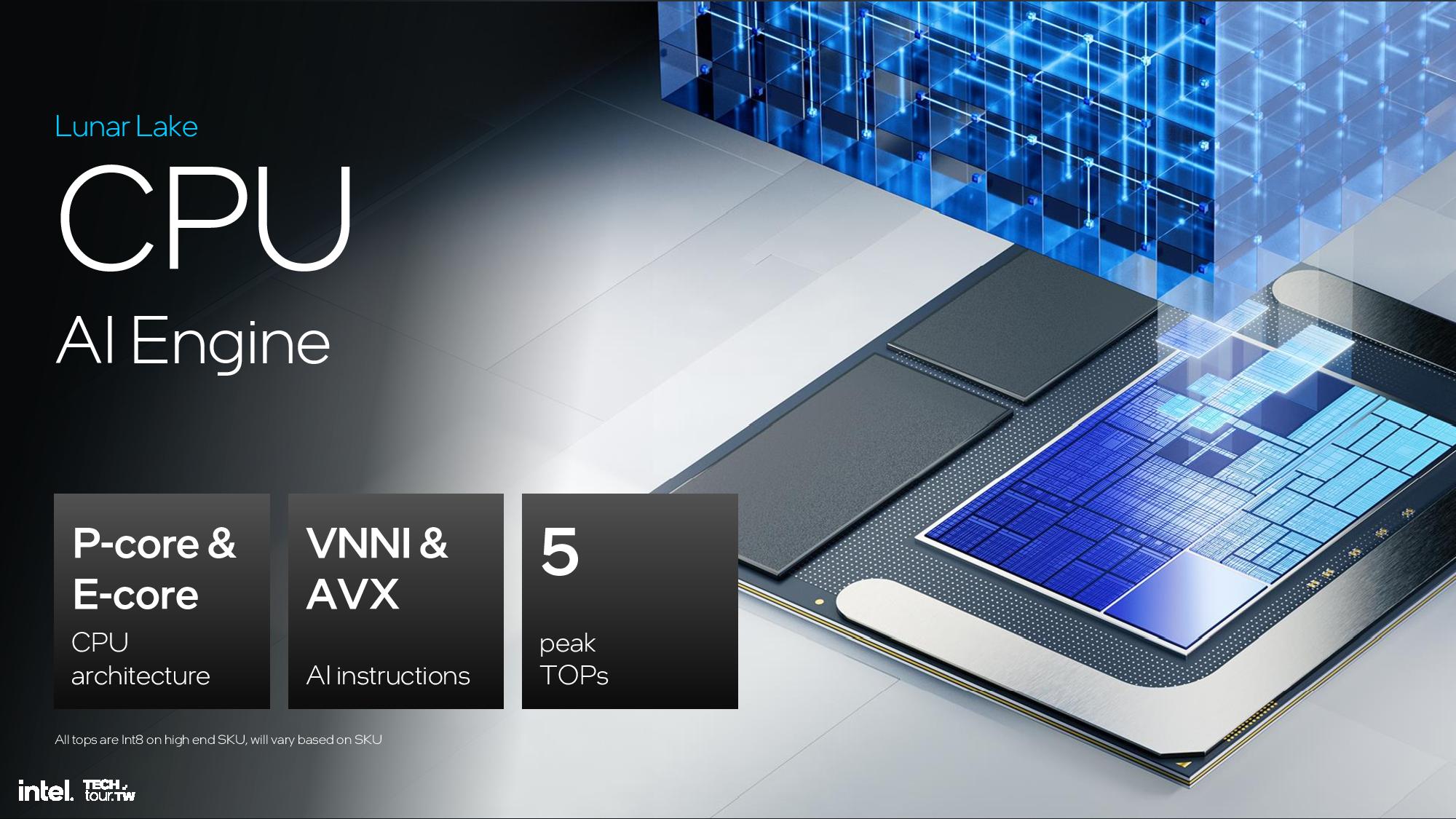
Every component of the Lunar Lake architecture has been optimized for a refined blend of power and performance that intel says will redefine what we expect from x86 PCs. Some of the biggest improvements come in the E-cores, with 38% and 68% IPC gains in the new Skymont architecture. There's also a 14% IPC gain for the Lion Cove P-cores — though these projections come with caveats. Graphics will see a 50% improvement in iGPU performance with the new Xe2 integrated graphics engine.
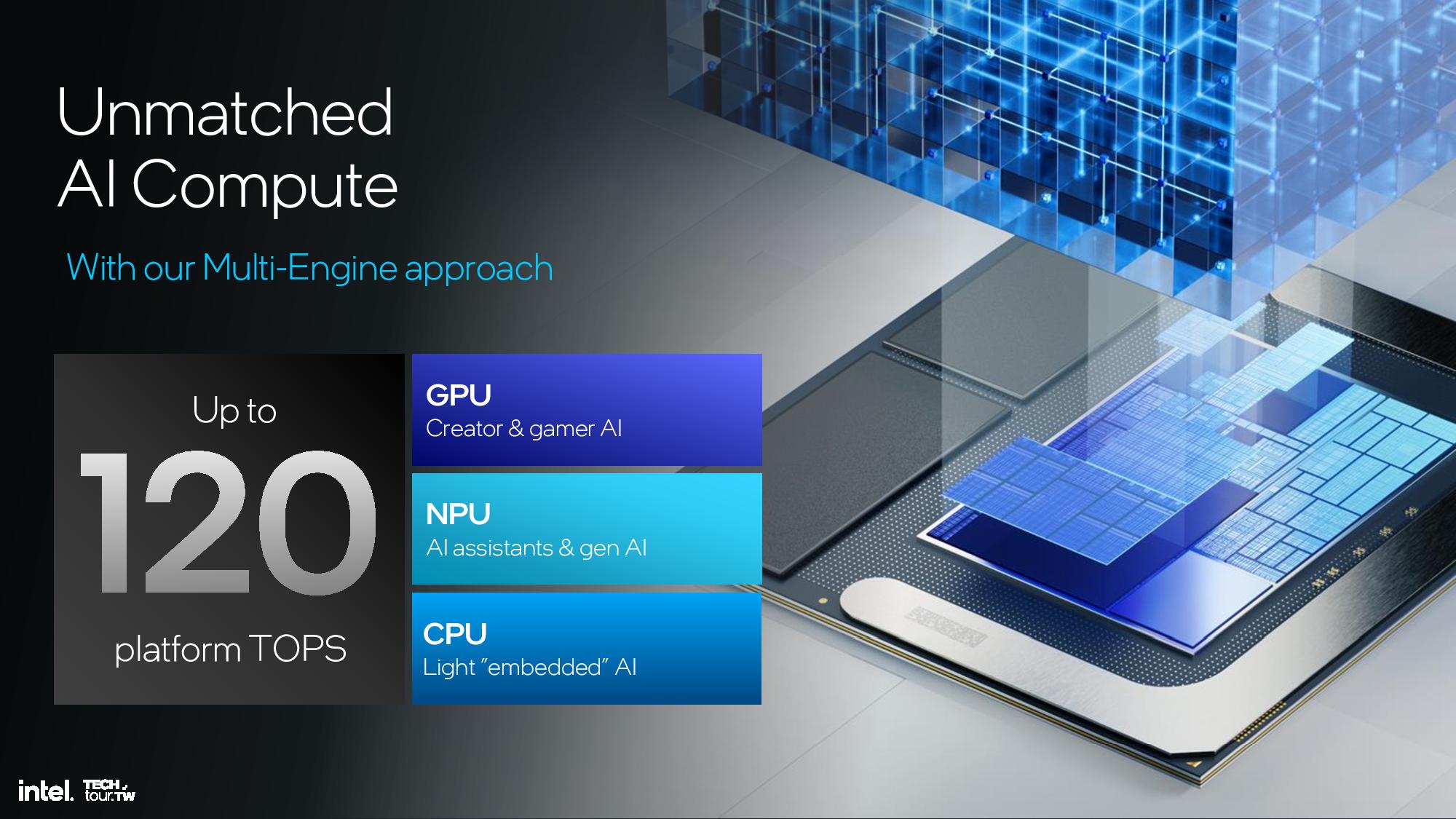
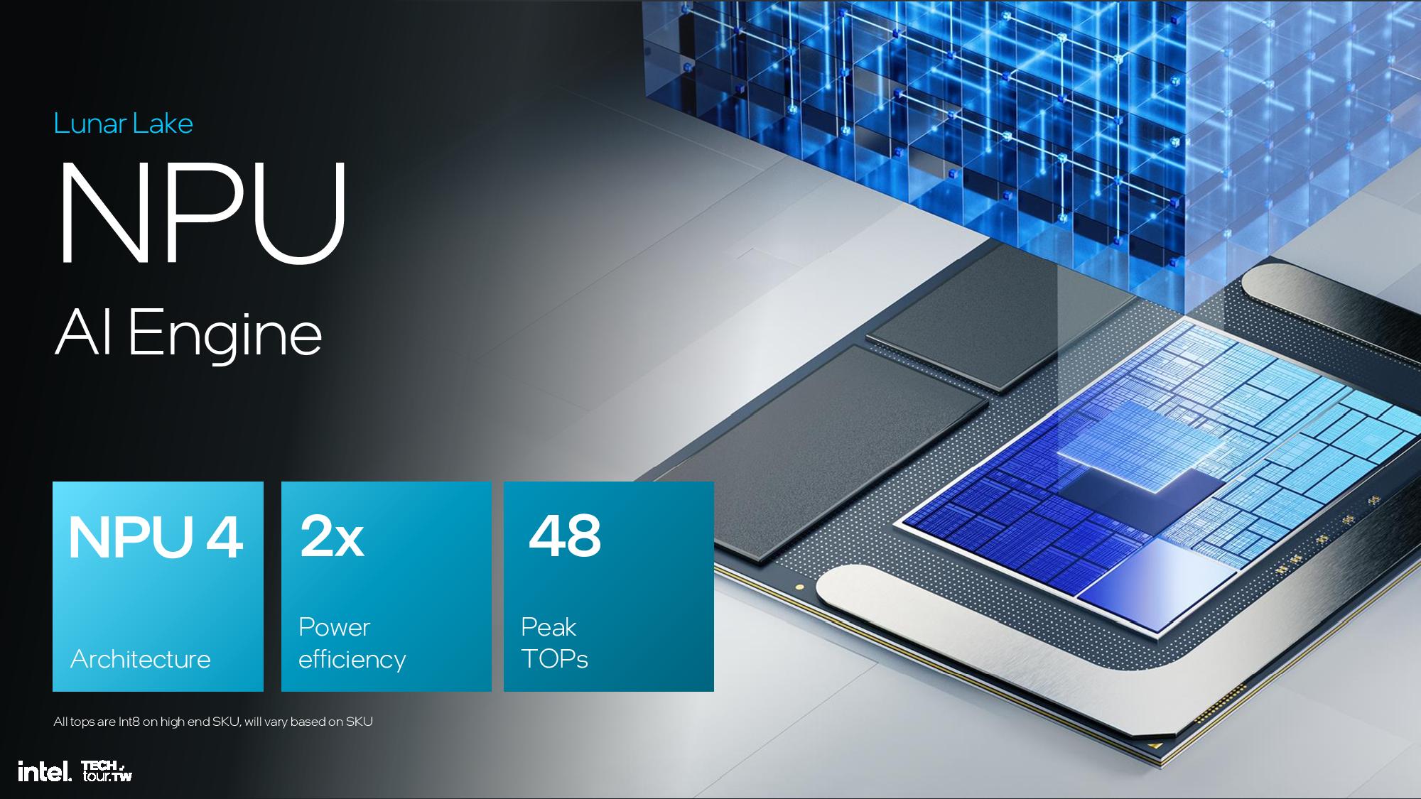
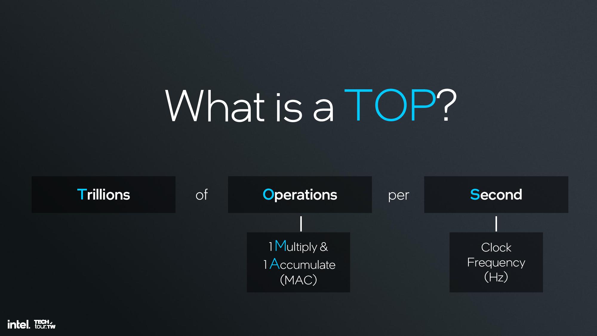
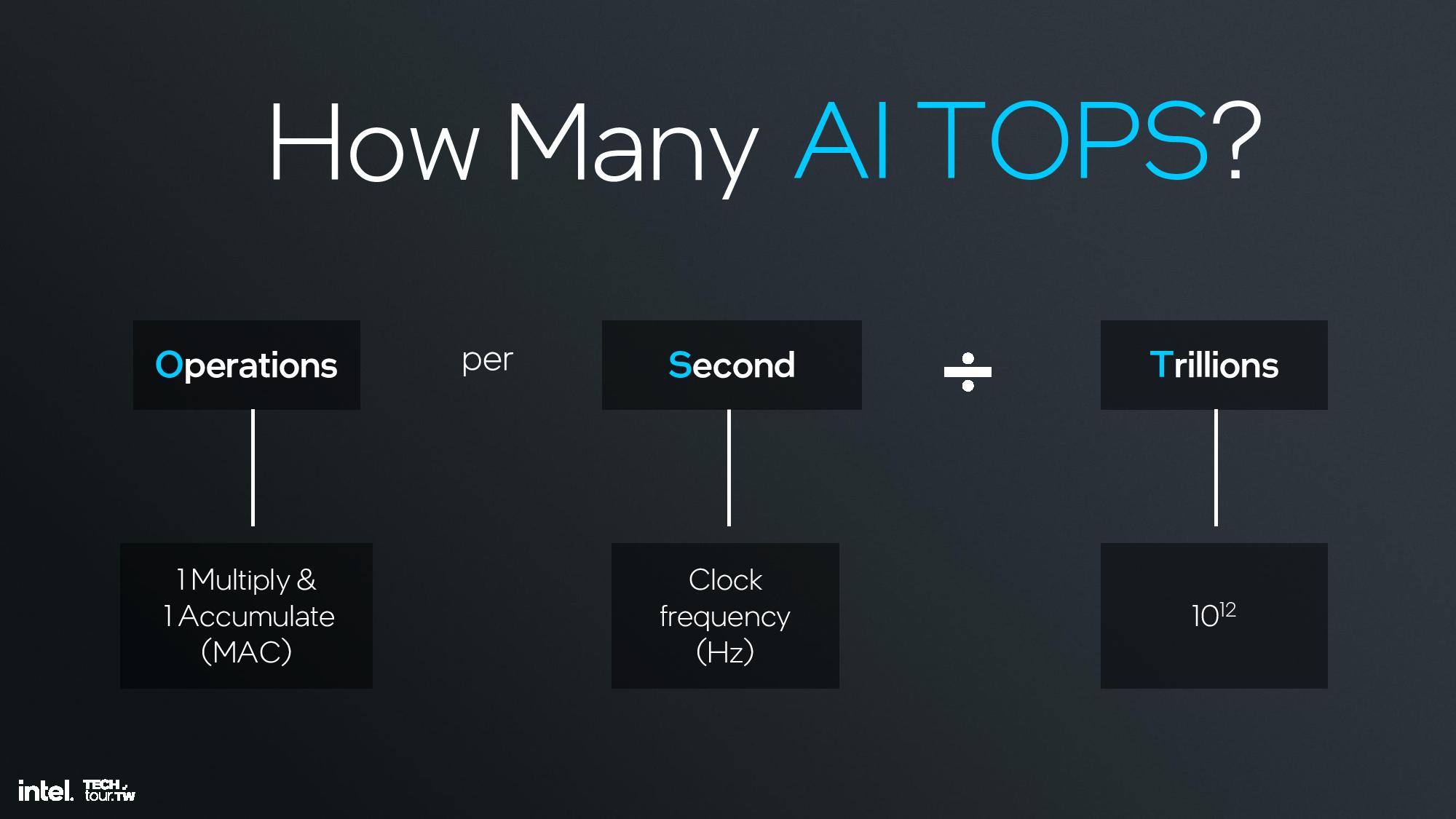
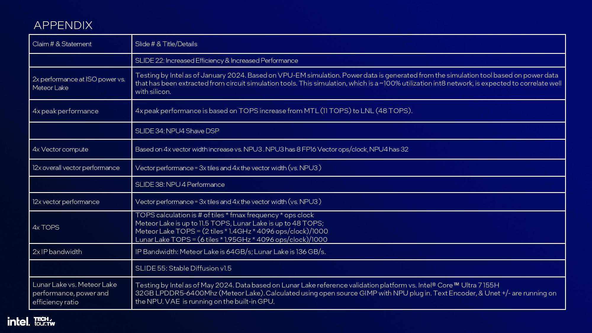
Lunar Lake incorporates Intel’s new neural processing unit (NPU) for AI workloads that delivers 48 TOPS of performance, easily providing enough performance to satisfy Microsoft’s requirement of 40 NPU TOPS for next-gen AI PCs. In fact, the Lunar Lake platform has far more AI performance under the hood — in total, it offers 120 TOPS when factoring in the CPU and iGPU.
The resulting Lunar Lake mobile chips employ an entirely new design methodology that focuses on ensuring power efficiency as a first-order priority, and this base architecture will be used as the building block for Intel’s future products, like Arrow Lake and Panther Lake. This new design focus is key to fending off a bevy of strong competitors in the laptop market from AMD, Apple, and now Qualcomm.
Surprisingly, intel turned to TSMC for its leading-edge 3nm N3B process node for its compute tile, which houses the CPU, GPU and NPU. It also uses the TSMC N6 node for the platform controller tile that houses the external I/O interfaces. In fact, the only Intel-fabbed silicon on the chip is the passive 22FFL Foveros base tile that facilitates communication between the tiles and the host system.
Intel says it chose TSMC’s nodes because they were the best available when the company began designing the chip, a nod to its delays on the manufacturing side of the operation as it looks to regain its lead in foundry technology through its five nodes in four years initiative. However, Intel designed the architectures to be easily portable to other process nodes, so we can expect it to return to using its own nodes with many of these same architectures in its future products.
Lunar Lake’s new microarchitectures pave the way for the company’s soon-to-be-announced Arrow Lake processors for the desktop, and even its Xeon 6 lineup, too. Let’s dive into the details.
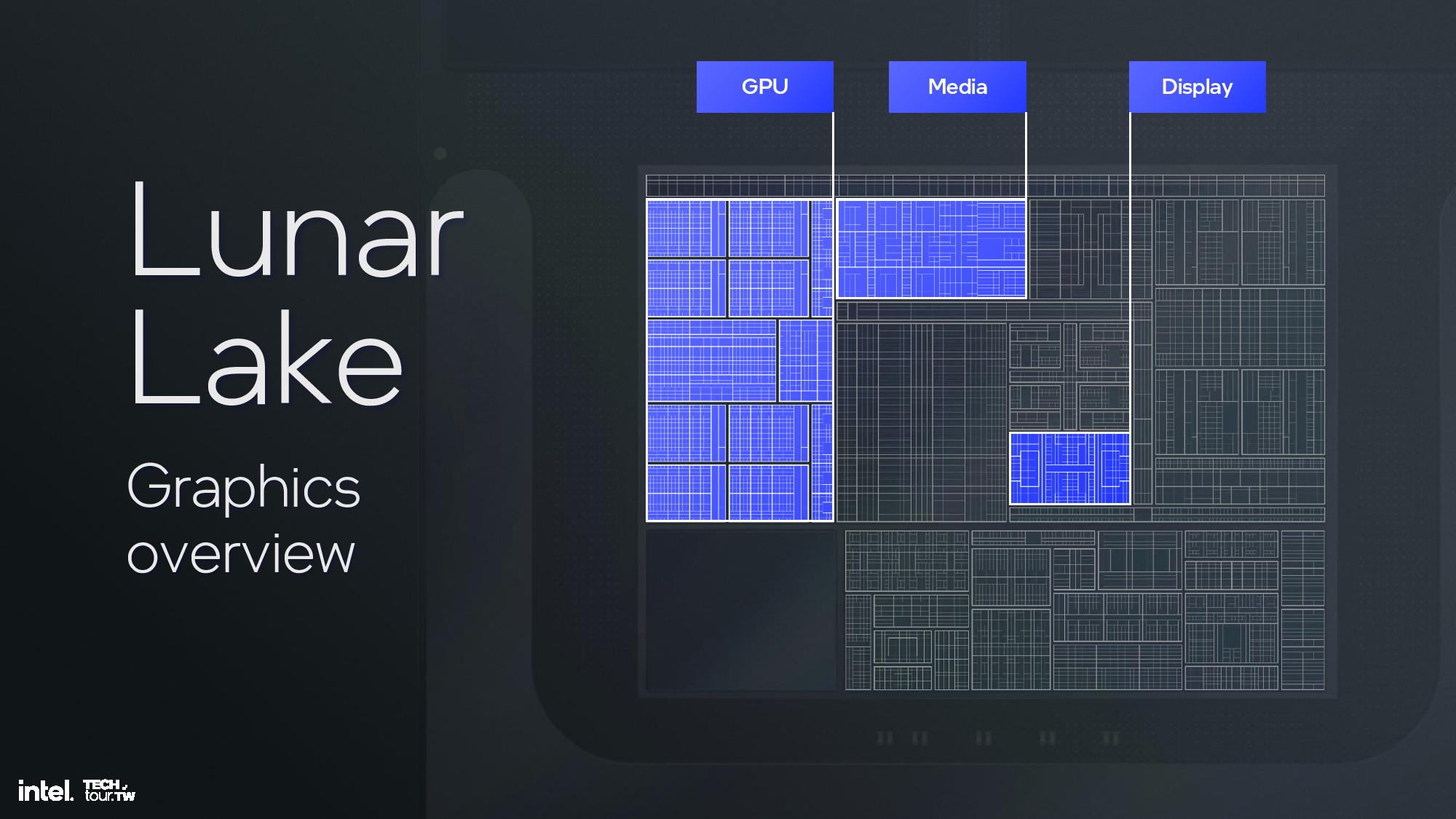
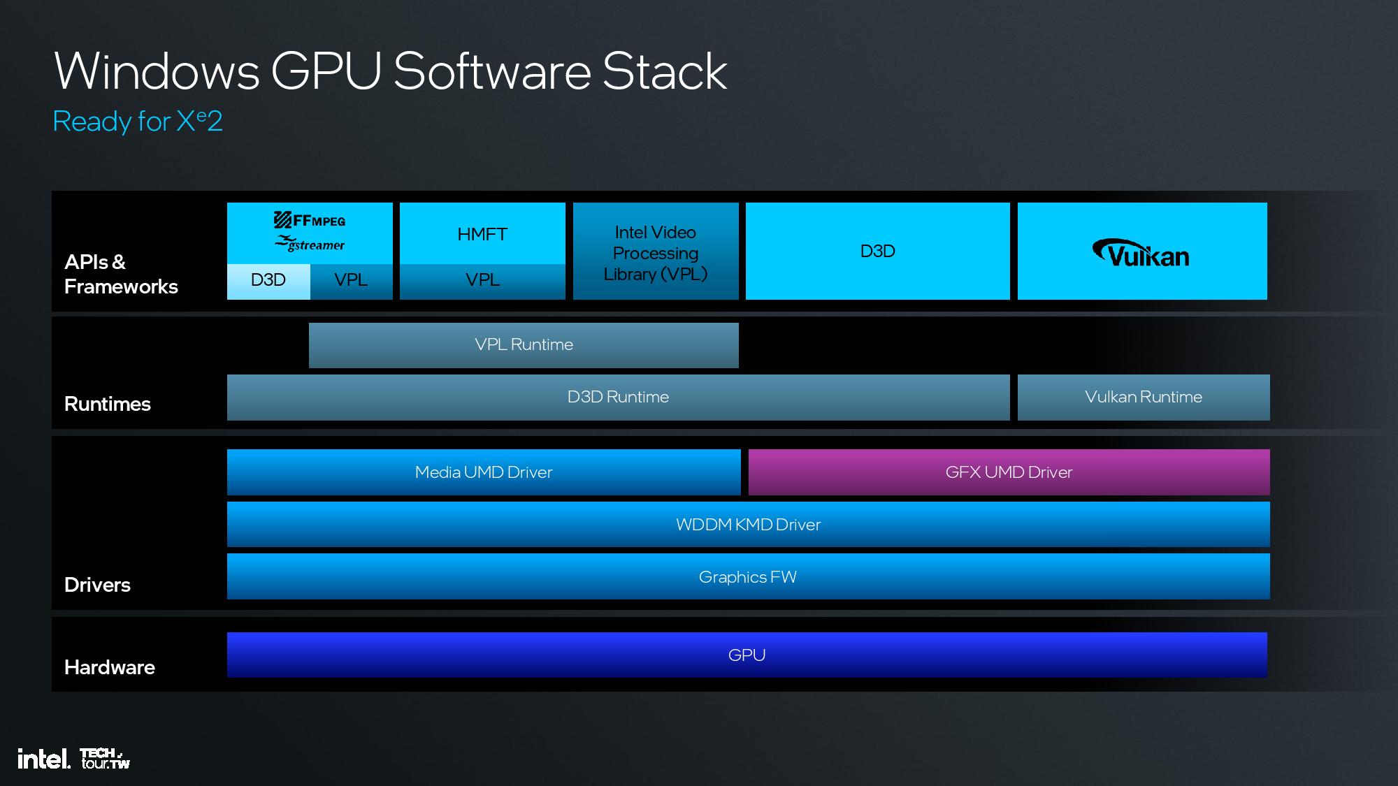
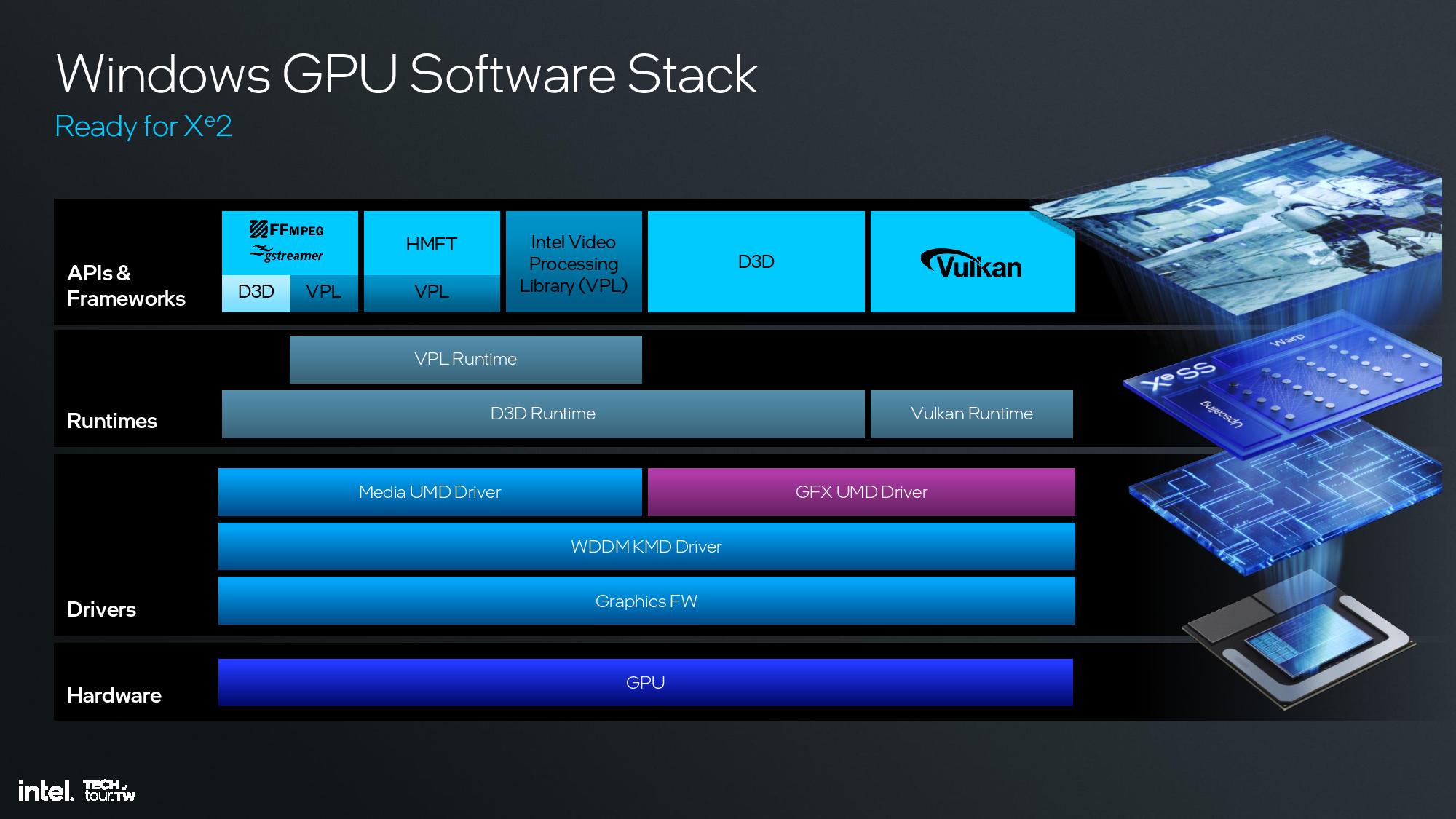
Lunar Lake SoC Overview
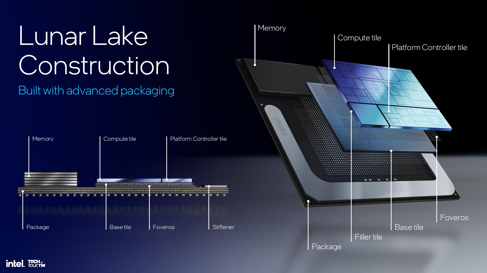
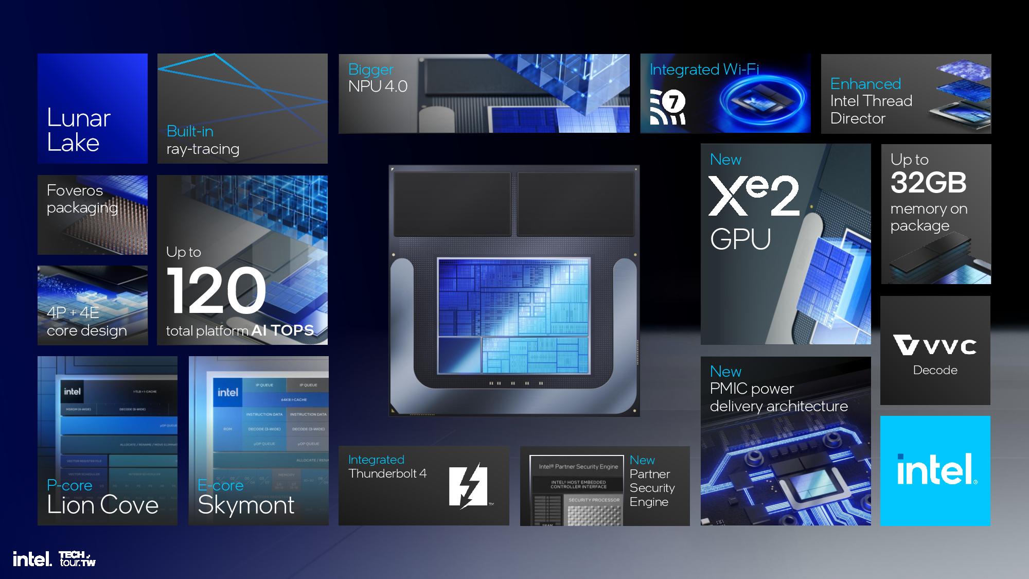
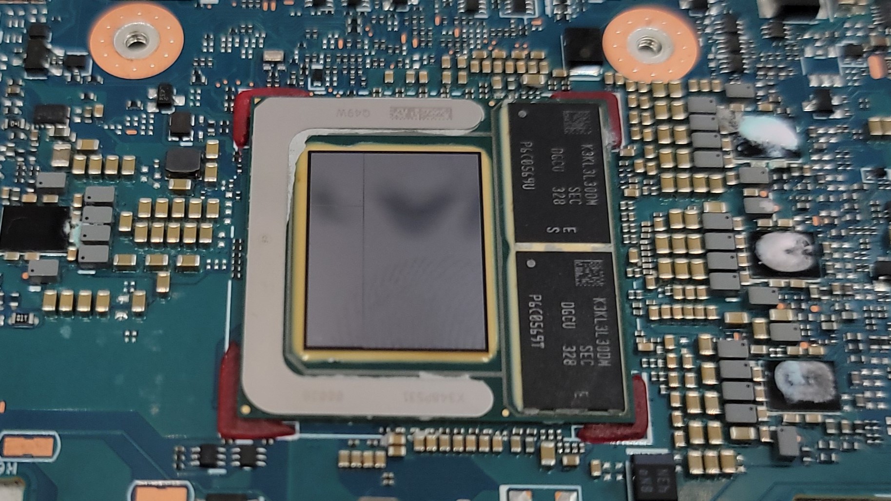
Intel’s Lunar Lake will come with four P-cores and four E-cores in the top-tier SKU. The chip is comprised of two logic tiles, a TSMC N3B compute tile and an N6 platform controller tile, along with a stiffener (a non-functional piece of filler silicon) placed atop a 22FFL base Foveros tile. The logic tiles are connected to the base tile with solder bonding with a 25-micron bump pitch (a critical measurement of interconnect density), an improvement over the 36-micron pitch used for Meteor Lake. This smaller pitch enables denser communication pathways between the units and helps reduce power consumption.
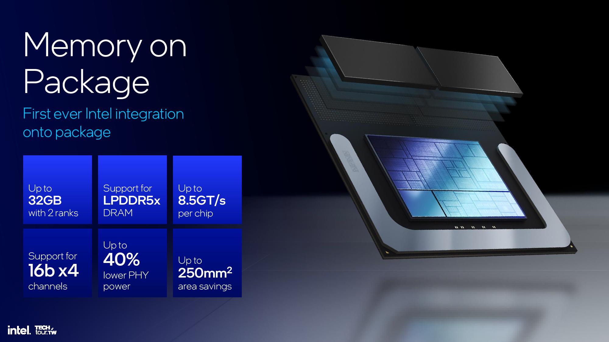
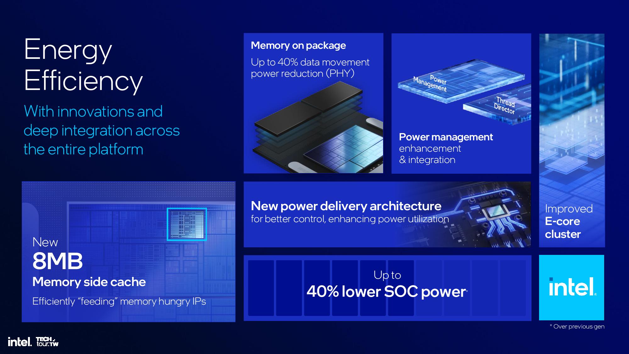
Intel places two stacks of LPDDR5X-8500 memory directly on the chip package, in 16GB or 32GB configurations, to reduce latency and board area while lowering the memory PHY’s power consumption by up to 40%. The memory communicates over four 16-bit channels and delivers up to 8.5 GT/s of throughput per chip.
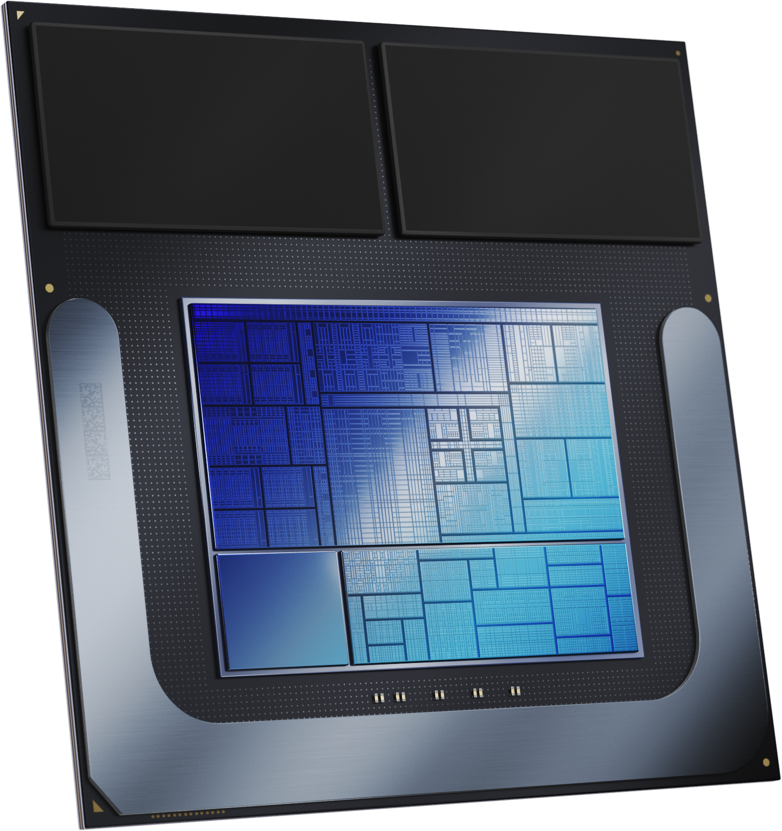
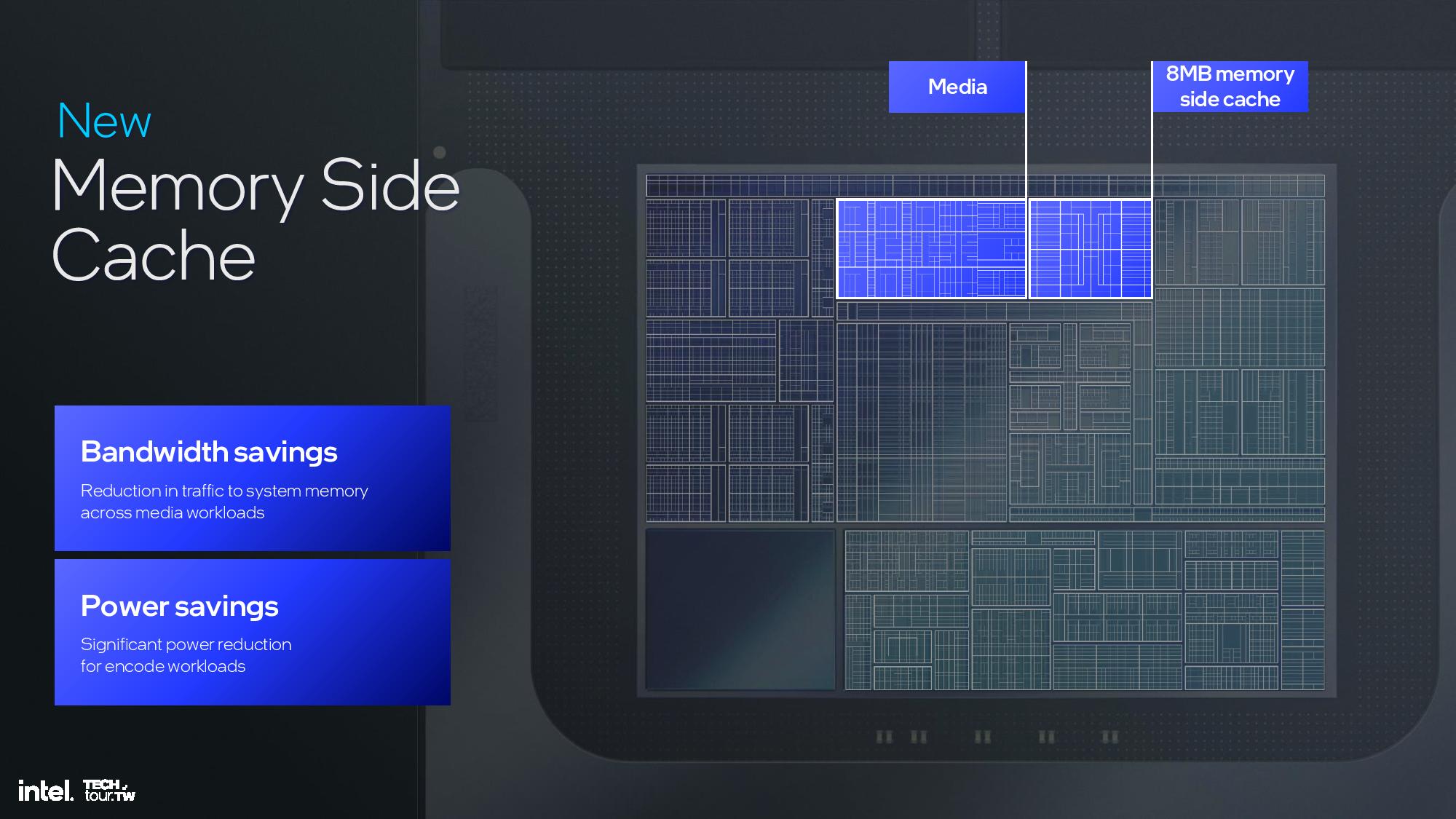
The compute tile houses the CPU P- and E-cores, Xe2 GPU, and NPU 4.0. It also incorporates a new 8MB ‘side cache’ that can be shared among all the various compute units to improve hit rates and reduce data movement, thus saving power. However, it doesn’t technically fit the definition of an L4 cache because it is shared between all of the units.
Intel has also moved the power delivery subsystem from the chip to the board, with four PMICs spread across the motherboard to provide multiple power rails and increased control. Overall, Intel claims a 40% reduction in SoC power over Meteor Lake.
Let’s dive into the core microarchitecture for the CPU, GPU and NPU, along with details about the platform controller tile, on the following pages.
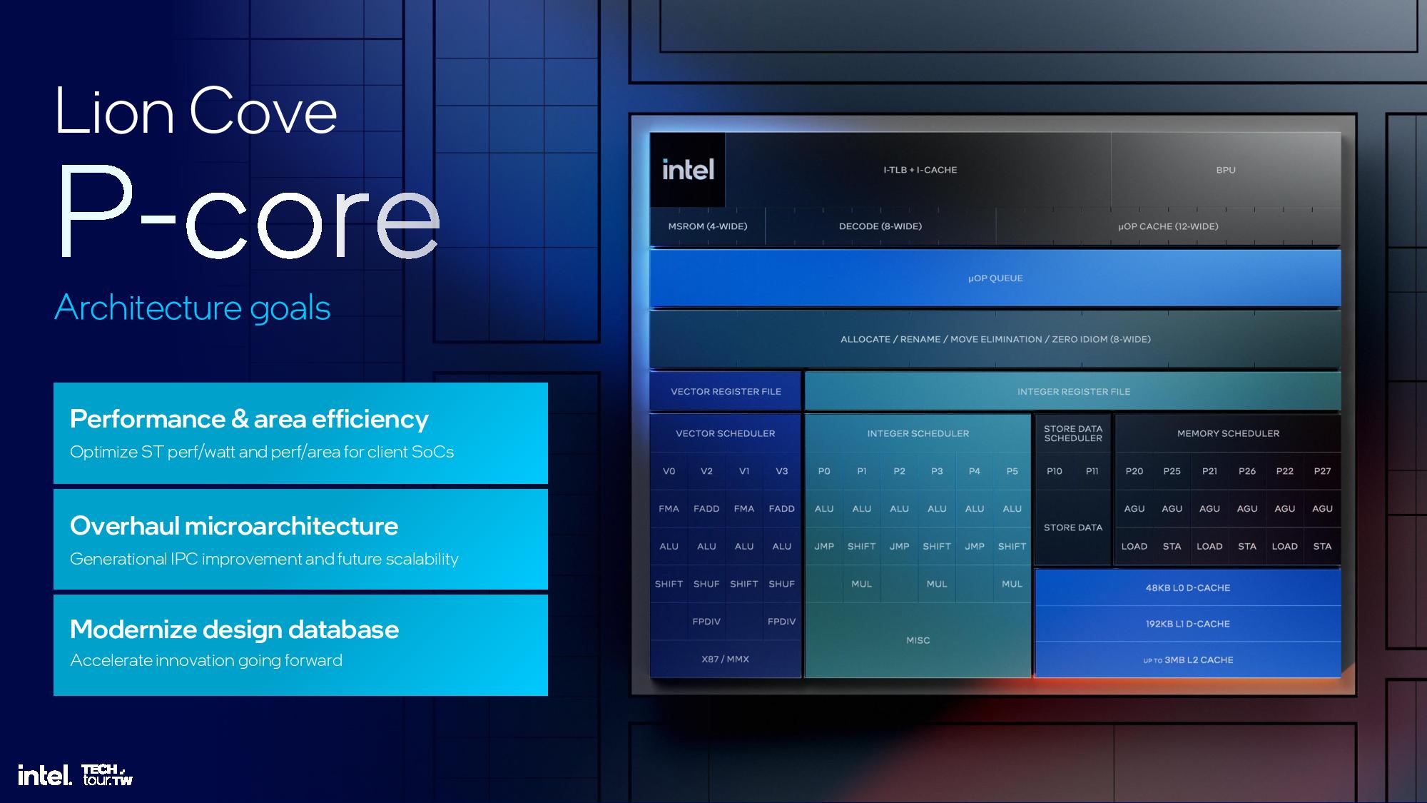
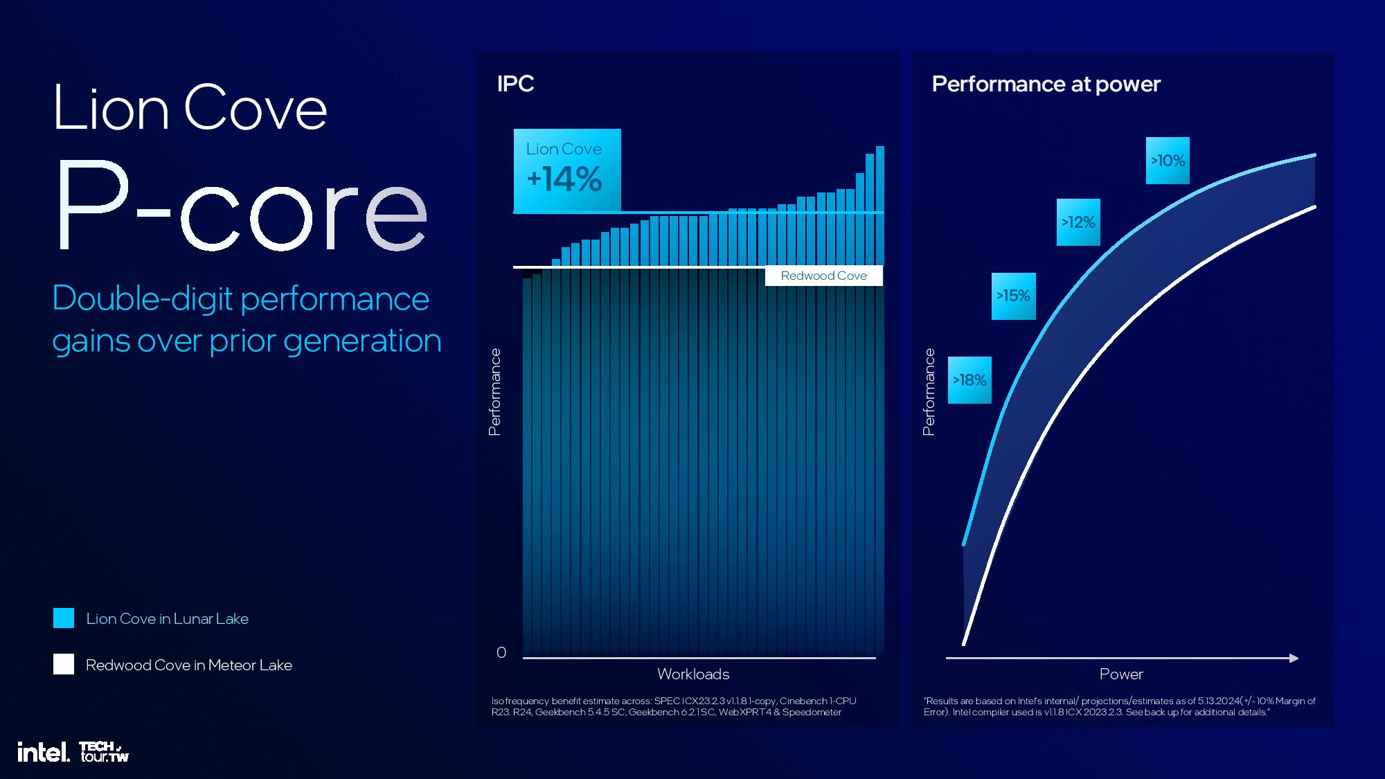
Lunar Lake’s P-cores deliver a 14% average gain in IPC (Instructions Per Cycle), which floats all boats in terms of performance. However, Intel took an unexpected turn in optimizing the cores for a hybrid architecture by removing hyperthreading and all the logic blocks that enable that performance-boosting feature.
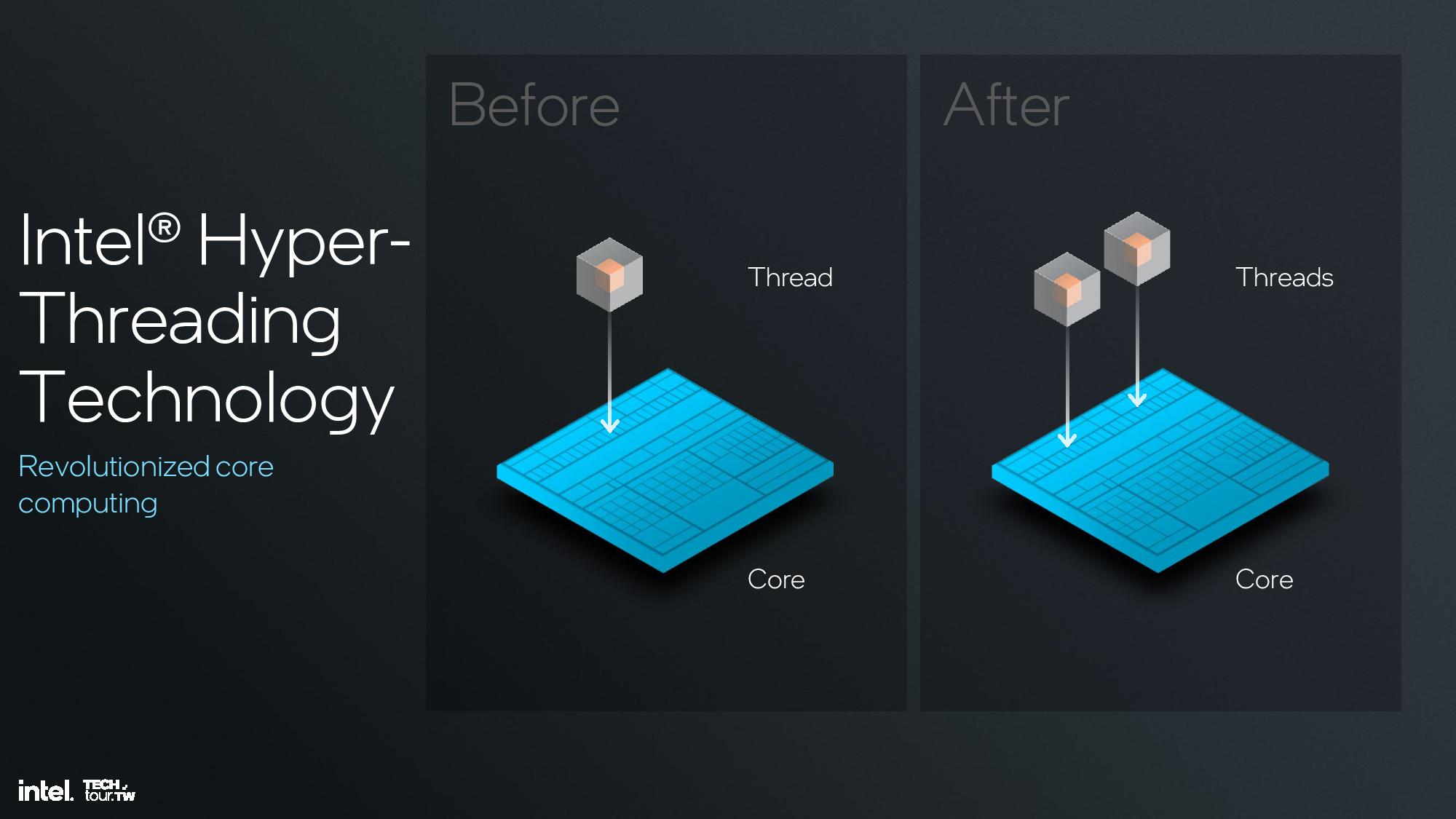
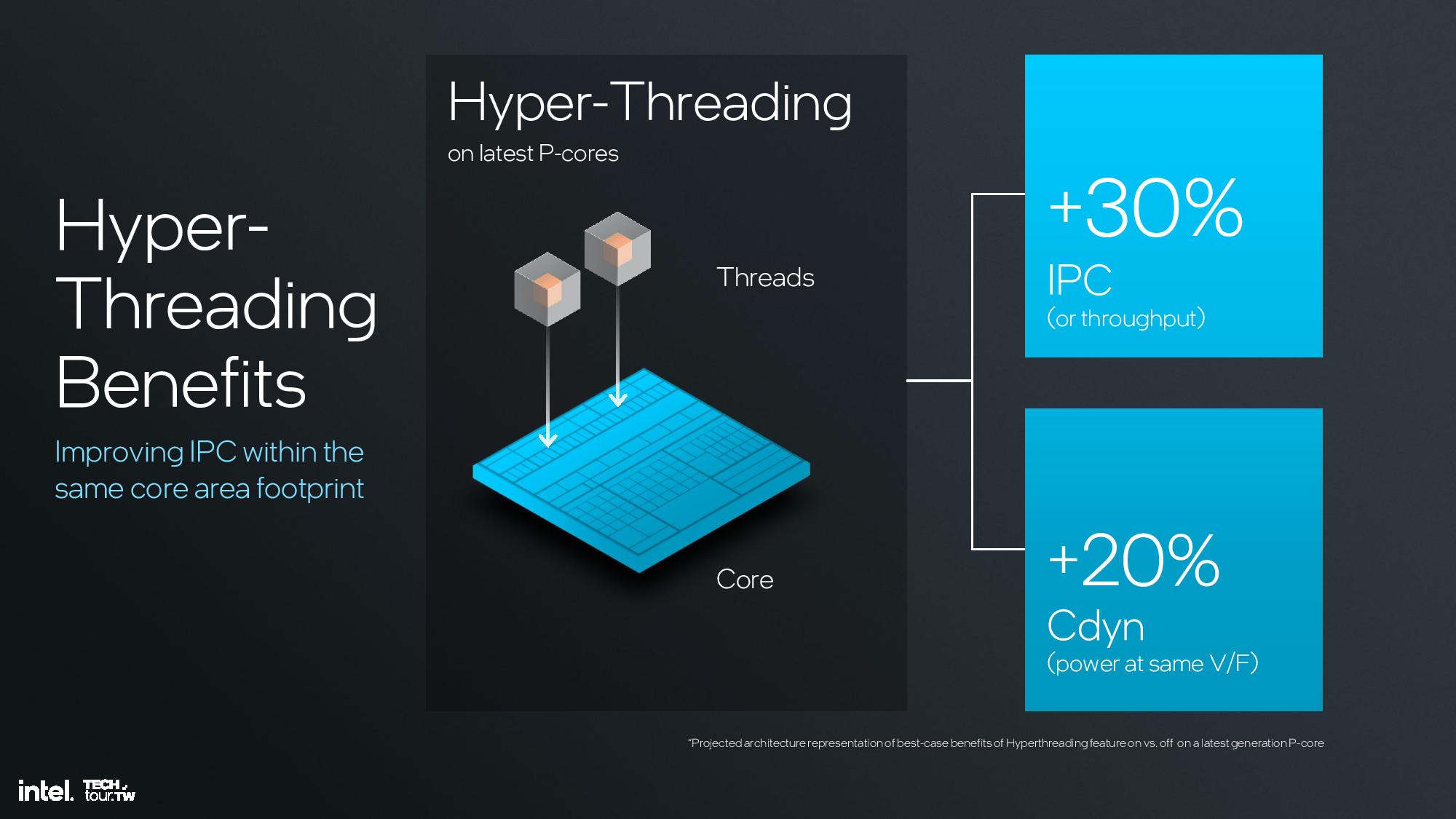
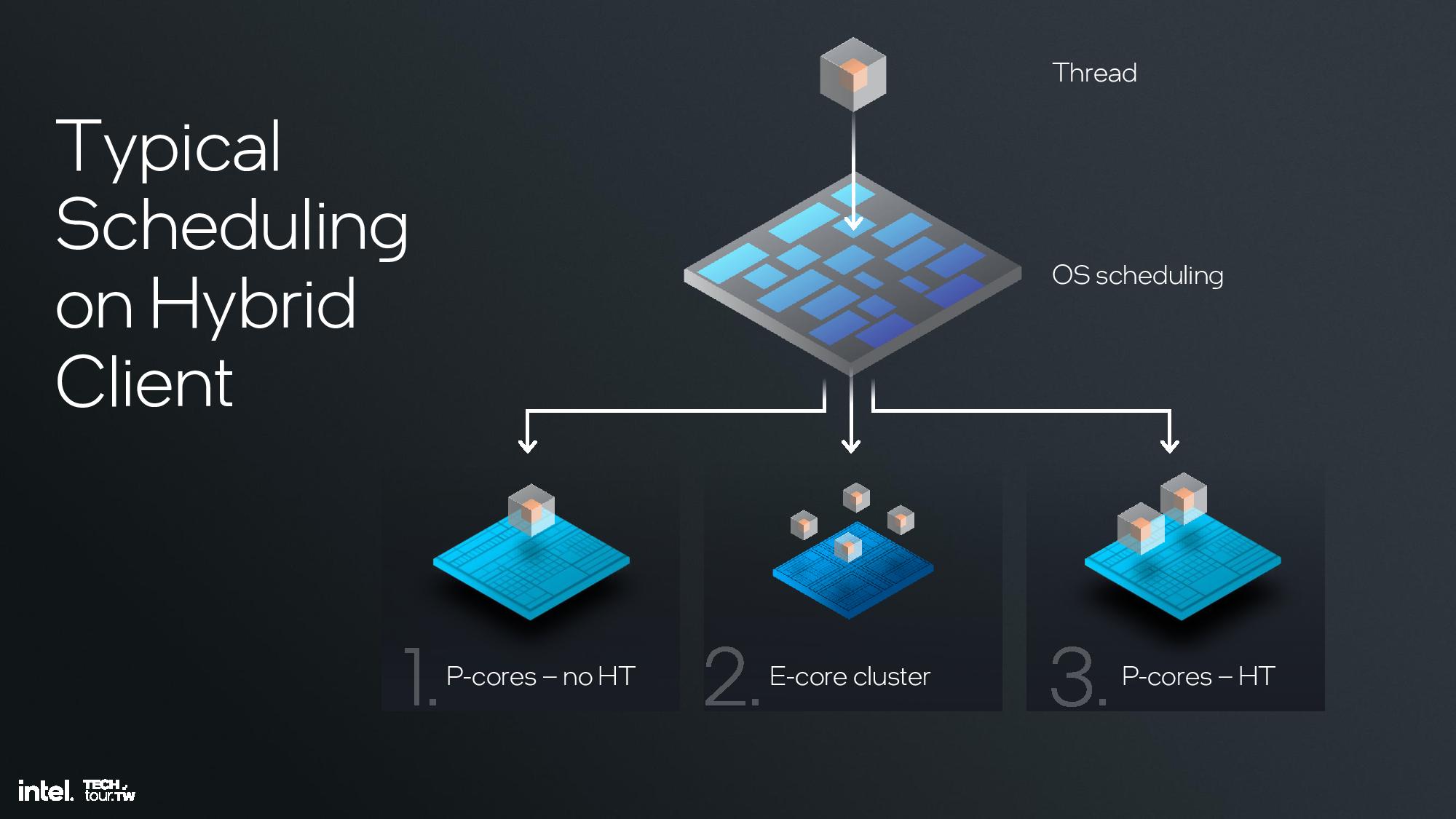
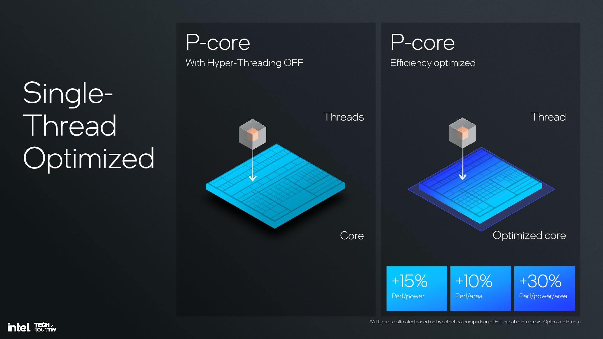
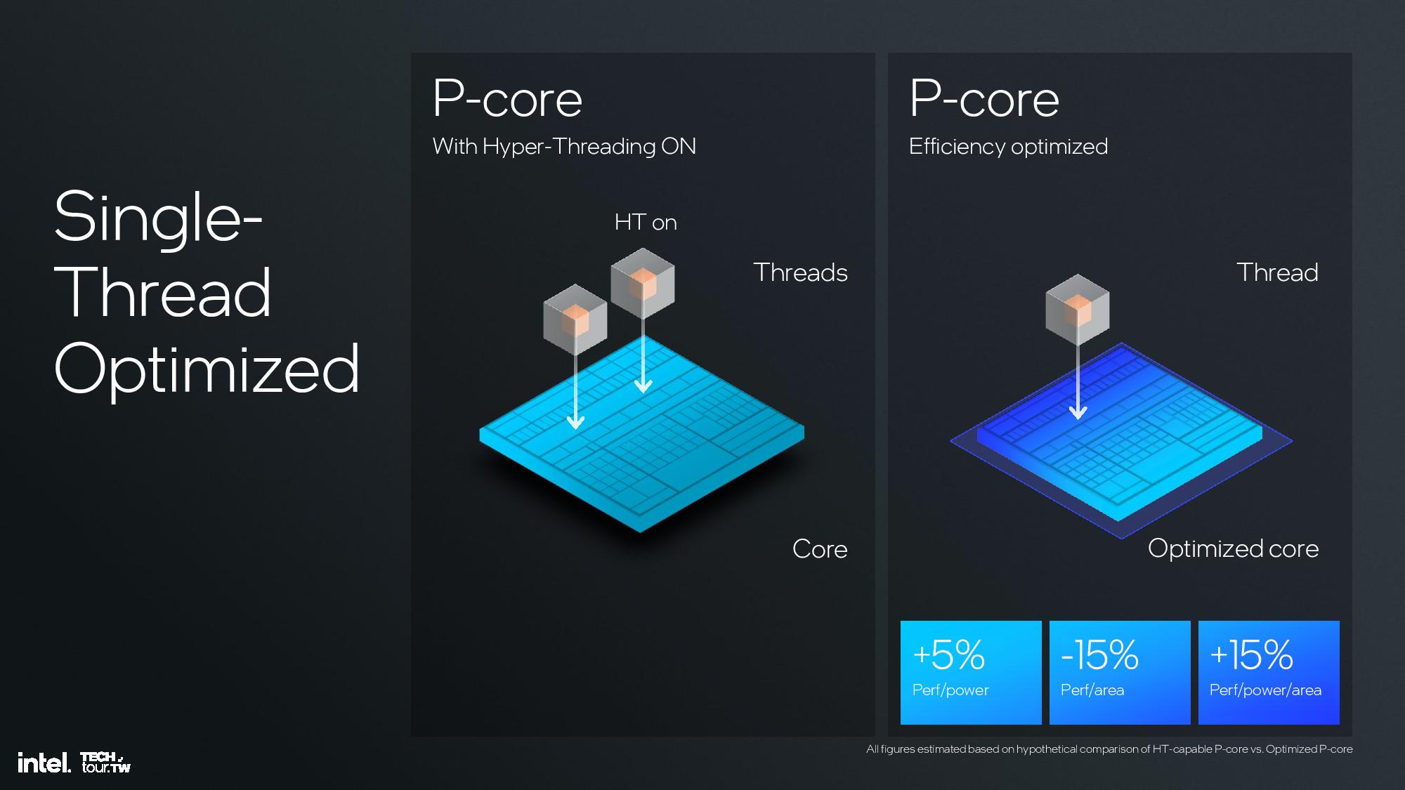
Intel’s architects concluded that hyperthreading, which boosts IPC by ~30% in heavily threaded workloads, isn’t as relevant in a hybrid design that leverages the more power- and area-efficient E-cores for threaded workloads. In fact, threads were typically scheduled into all P-cores first without leveraging the extra threads on the cores, and then spilling additional threads spill over to the E-cores. Only after the E-cores were saturated did additional threads begin to get scheduled into the extra threads available on the P-cores.
Removing the dedicated fairness mechanisms and extra security features required for hyperthreading makes the core leaner, delivering a 15% increase in performance efficiency, 10% increase in performance per area, and a 30% improvement in performance per power per area. This was much more effective than merely disabling hyperthreading while leaving the control circuitry present, as shown in the measurements in the last slide above. The new approach also preserves die area for other additives, like more E-cores or GPU cores.
Intel isn’t discarding hyperthreading for all use-cases — it still sees tremendous value in P-core-only designs. As such, Intel architected two versions of the Lion Cove core, one with and one without hyperthreading, so that the threaded Lion Cove core can be used in other applications, like we see in the forthcoming Xeon 6 processors.
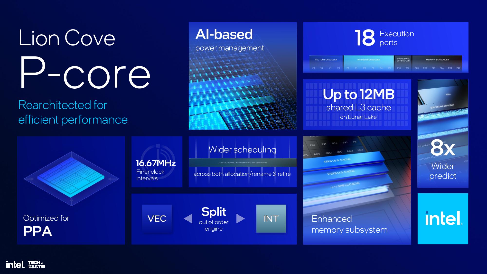
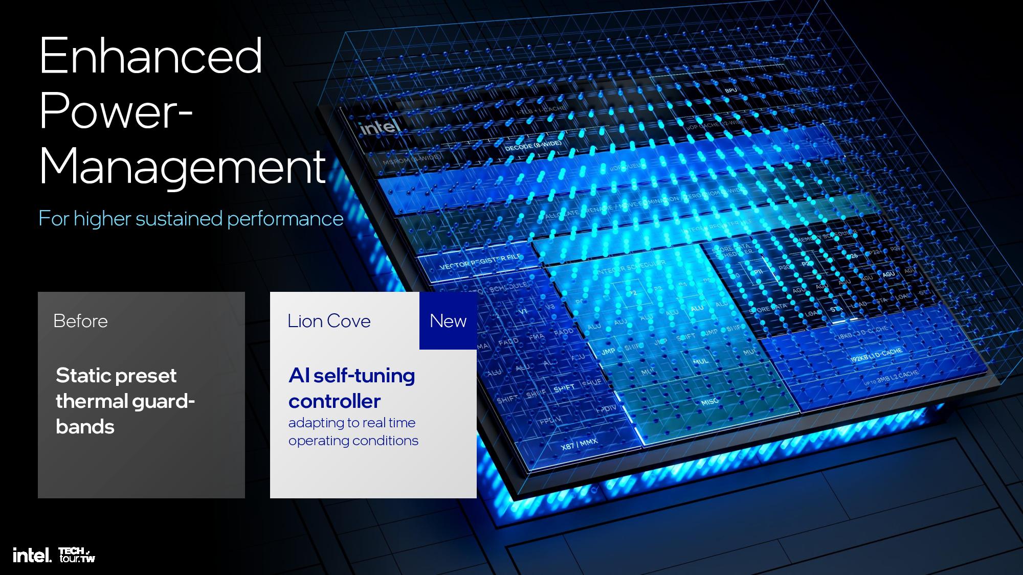
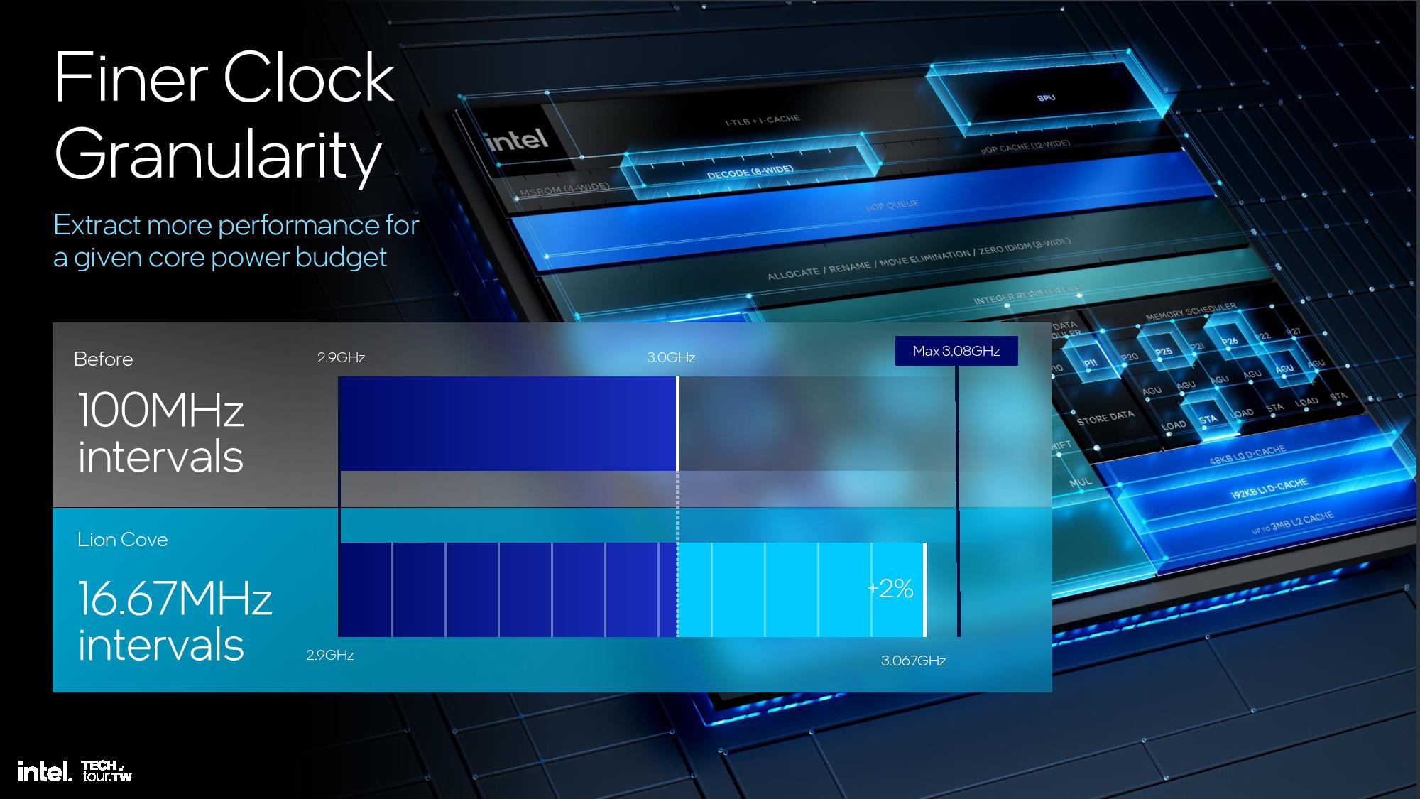
Lion Cove also marks a shift from pre-defined static settings for various operating conditions, such as assigning certain points on the voltage/frequency curve for different thermal and power thresholds. It now uses an AI self-tuning controller to dynamically adapt in a more intelligent manner. Intel’s clock frequencies also used to only be adjustable in 100 MHz increments (bins) but are now tunable in 16.67 MHz bins to provide more fine-grained frequency and power control. Intel credits this with single-digit percentage increases in either power efficiency or performance in some scenarios, and every bit counts in an efficiency-first architecture.
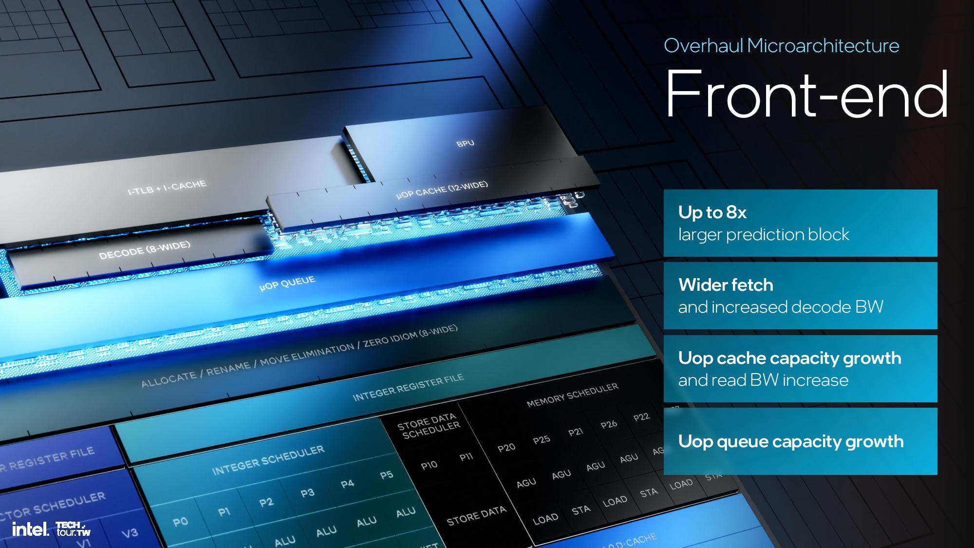
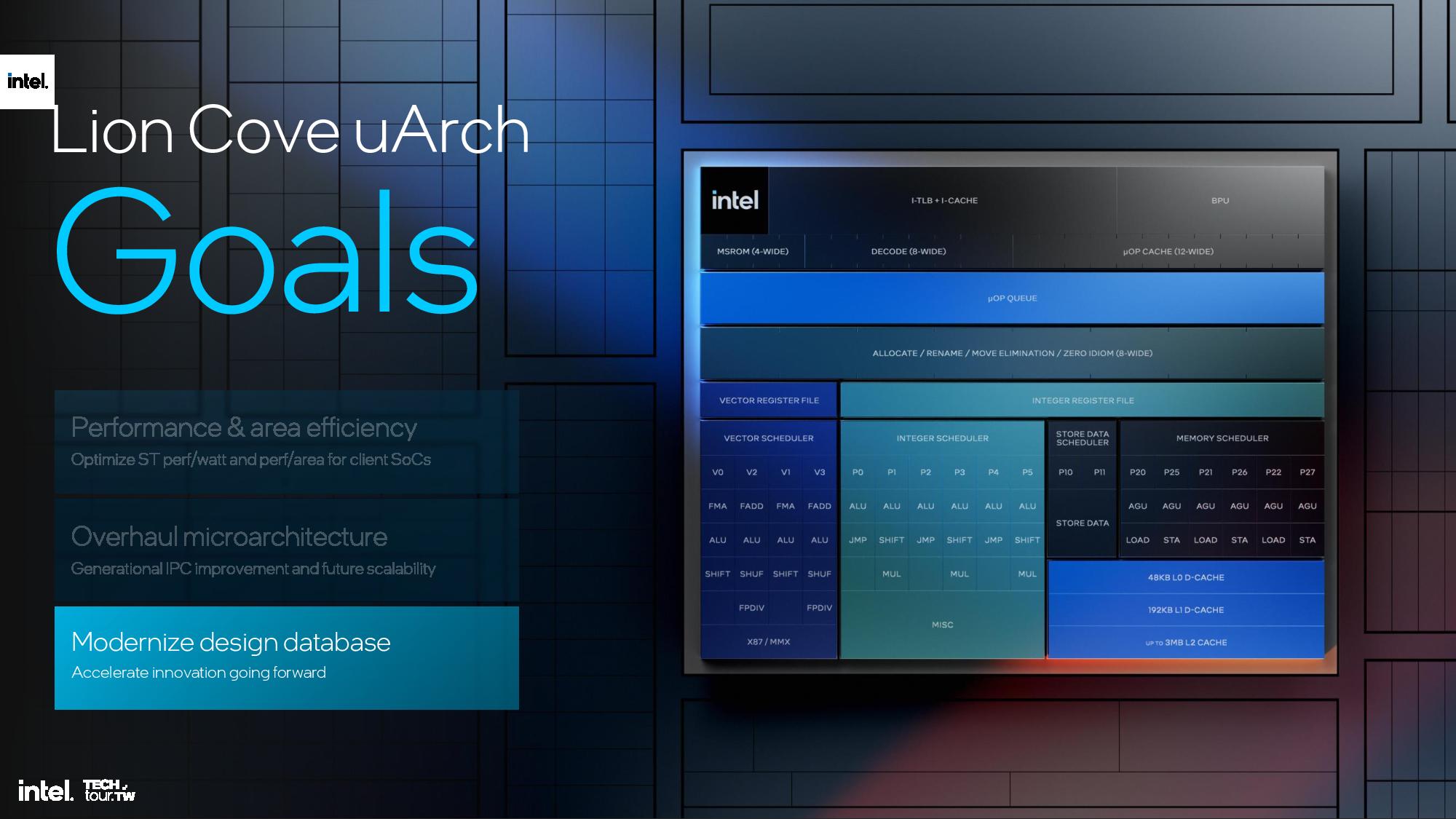
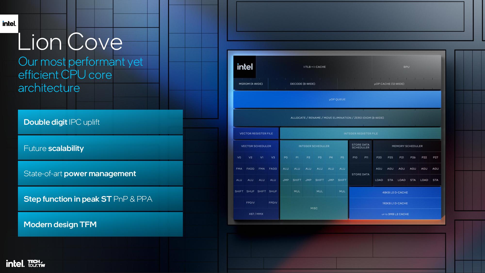

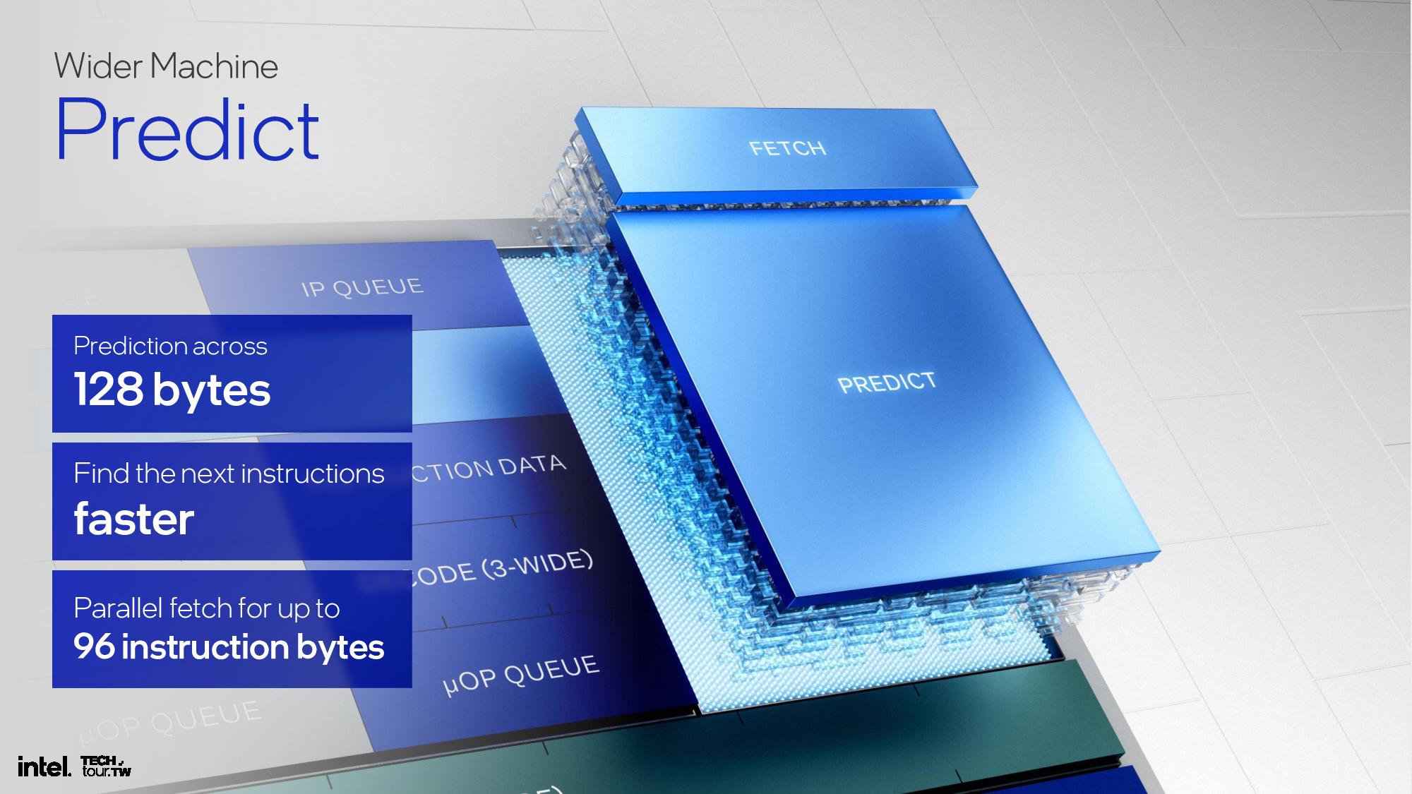
The front end of the microarchitecture fetches x86 instructions and decodes them into microoperations to feed the out of order execution engine. The goal is to saturate the out of order part of the engine to prevent stalls, and that requires fast and accurate branch prediction.
Intel says it widened the prediction block by 8X over the previous architecture while maintaining accuracy. Intel also tripled the request bandwidth from the instruction cache to the L2 and doubled the instruction fetch bandwidth from 64 to 128 bytes per second. Additionally, decode bandwidth was bumped up from 6 to 8 instructions per cycle while the micro-op cache was increased along with its read bandwidth. The micro-op queue was also increased from 144 entries to 192 entries.
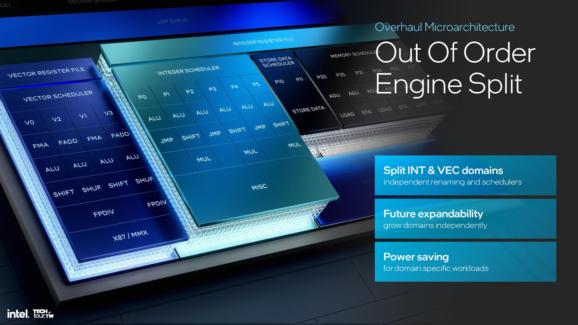
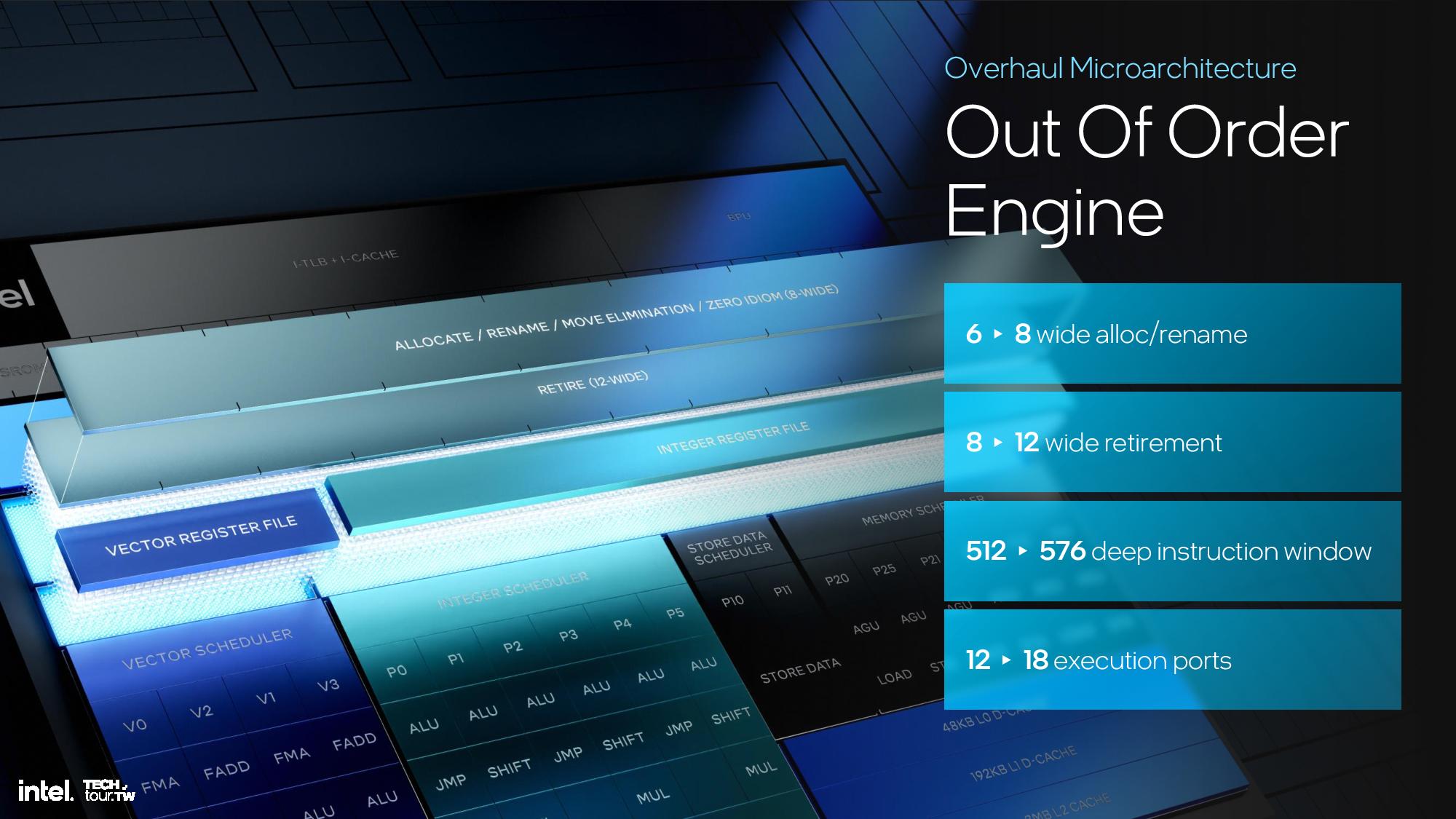
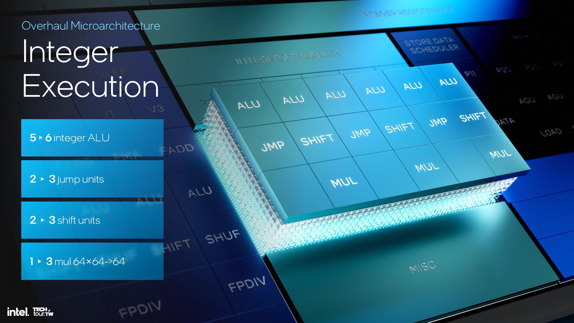
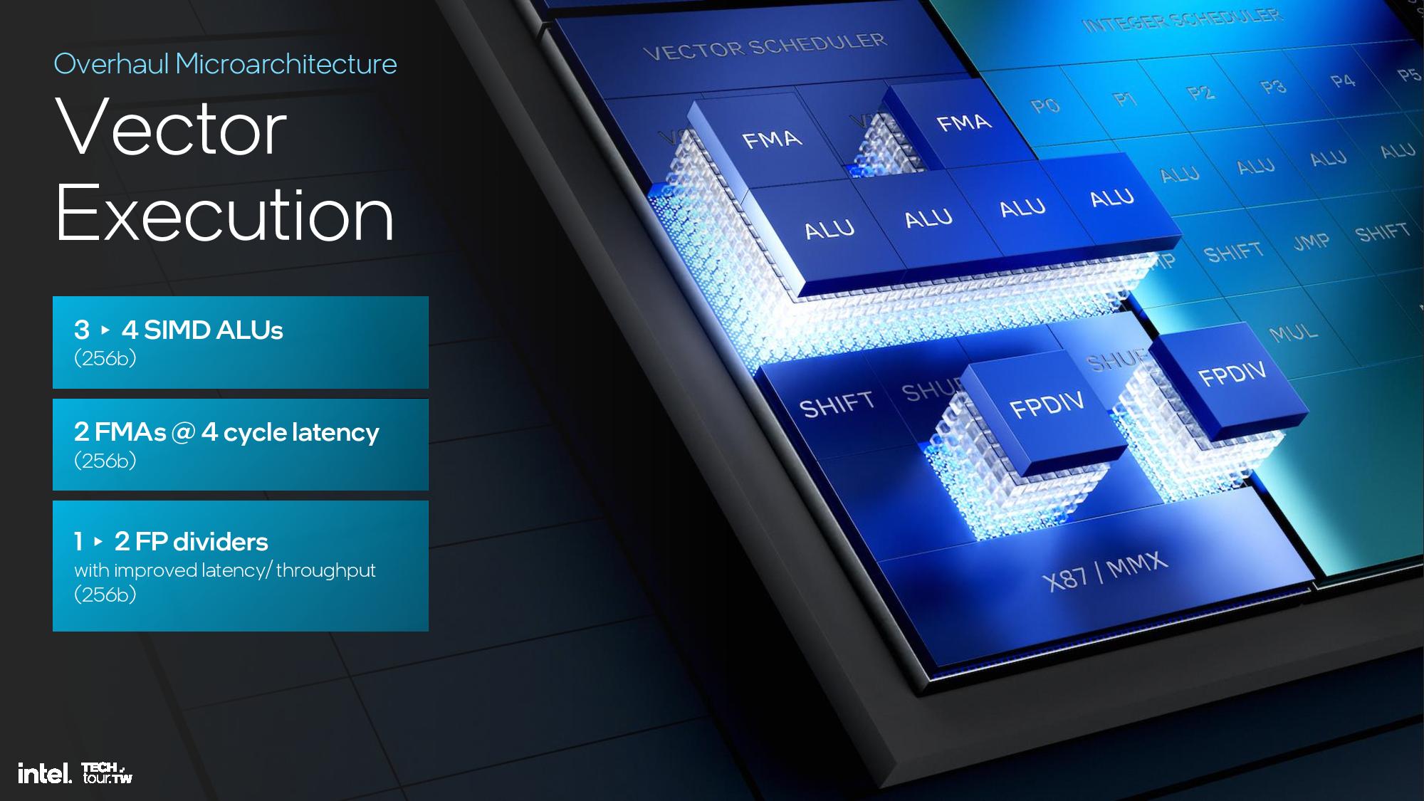
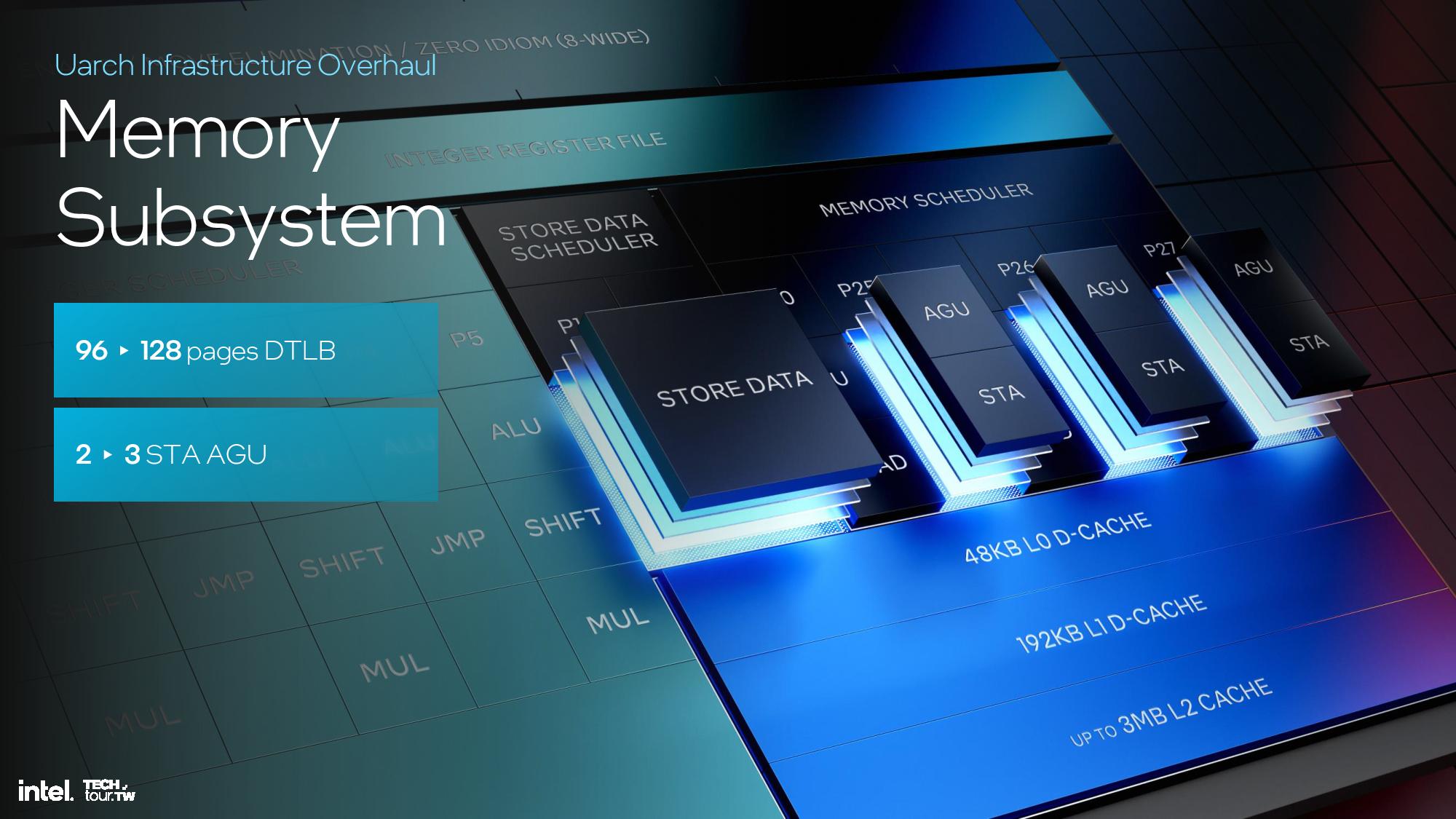
Previous P-core architectures had a single scheduler to dispatch instructions across the execution ports, but the design incurred hardware overhead and scalability issues. To address these issues, Intel split the out of order engine into integer and vector domains with independent renamers and schedulers to increase flexibility. A range of improvements were also made to the retirement, instruction window, and execution ports, along with other improvements to the integer and vector execution pipelines (listed in the slides).
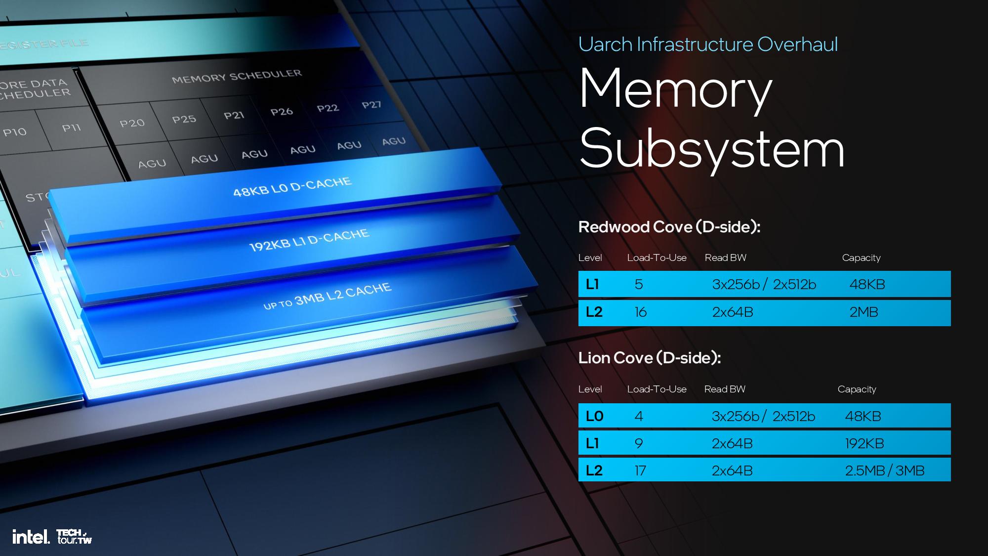
The memory subsystem has a new L0 cache level. The architects completely redesigned the data cache to add a 192KB tier between the existing L1 and L2 caches. This resulted in renaming the existing L1 as L0. Ultimately this decreases the average load-to-use time, which increases IPC, and enables increasing the L2 cache capacity without latency sacrifices due to the increased capacity. As a result, L2 cache grows to 2.5MB on Lunar Lake and 3MB on Arrow Lake (they both use Lion Cove for the P-cores).
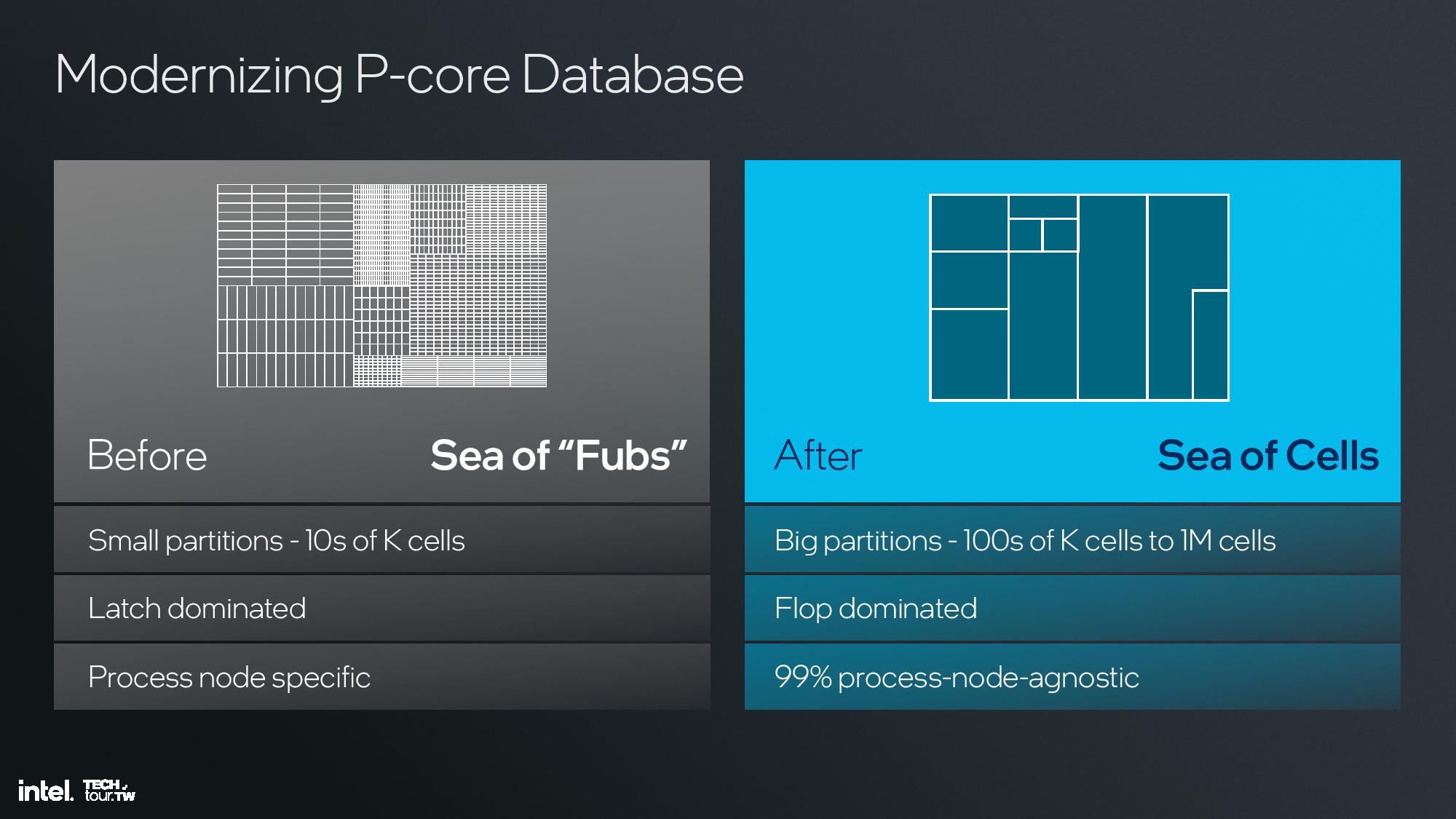
Intel also switched from using proprietary design tools to industry-standard tools optimized for its use. Intel’s old architectures were designed with “Fubs” (functional blocks) of tens of thousands of cells consisting of manually drawn circuits, but it has now moved to using big, synthesized partitions of hundreds of thousands to millions of cells. The removal of the artificial boundaries improves design time, increases utilization, and reduces area.
This also allowed for the addition of more configuration knobs into the design to spin off customized SoC-specific designs faster, with the lead architect saying this allows for more customization between the cores used for Lunar Lake and Arrow Lake. This design methodology also makes 99% of the design transferable to other process nodes, a key advance that prevents the stumbles we’ve seen in the past where intel’s new architectures were delayed by massive process node delays (as with 10nm, for instance).
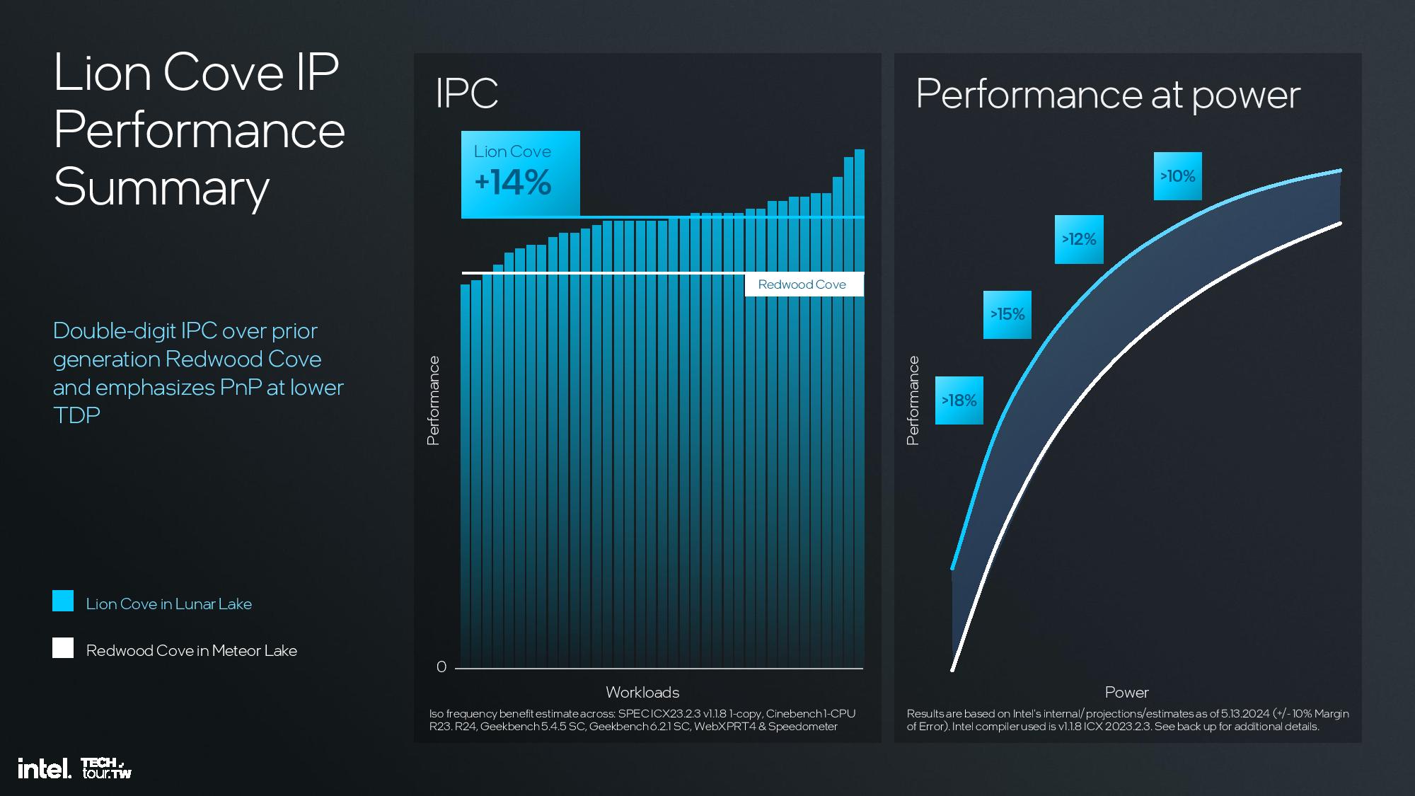
The end result of the changes is a 14% increase in IPC at a fixed clock rate over the previous-gen Redwood Cove architecture used in Meteor Lake. Intel also points to overall performance improvements that range from 10% to 18% over Meteor Lake depending upon the operating power of the chip. Notably, these power/performance improvements are based on projections/estimates, so Intel has given itself a +/- 10% margin of error for the metrics on the ‘performance at power’ chart.
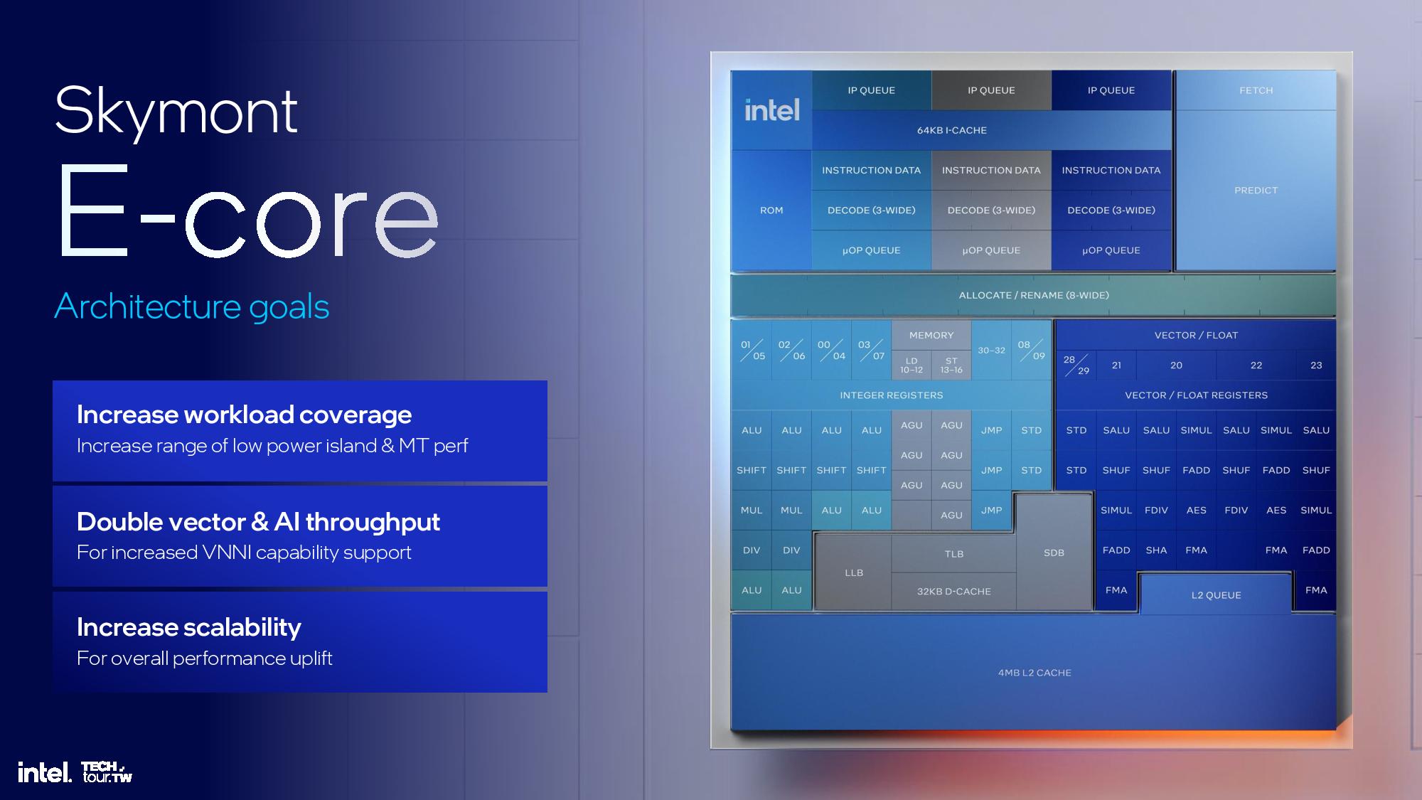
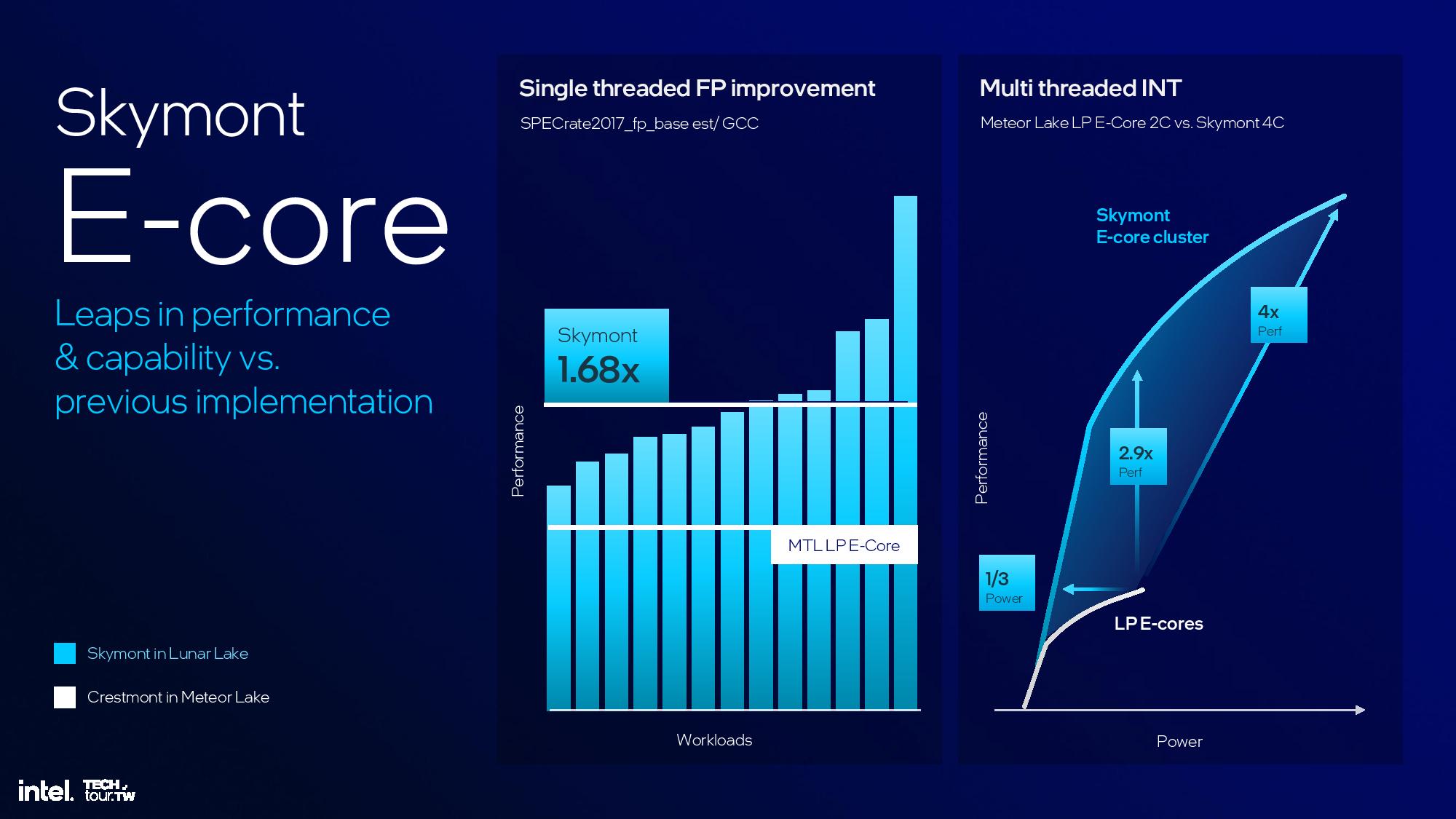
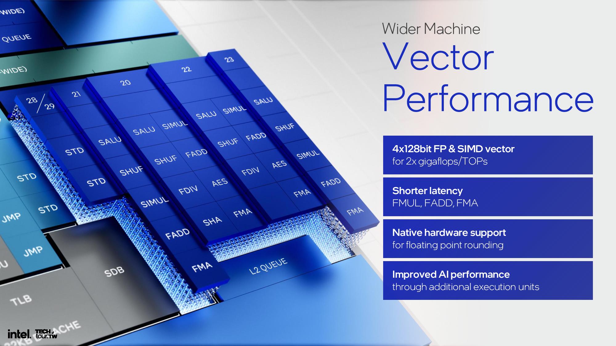
Lion Cove delivers an impressive number of improvements to the core microarchitecture, but Skymont sees an even bigger advance over the prior gen with a 38% IPC improvement in integer workloads and a 68% IPC gain in floating point work, fueling an up to 2x increase in single-threaded performance and up to 4x more peak performance in multi-threaded workloads than the Meteor Lake LP E-cores. Intel also doubled throughput in vectorized AVX and VNNI workloads.
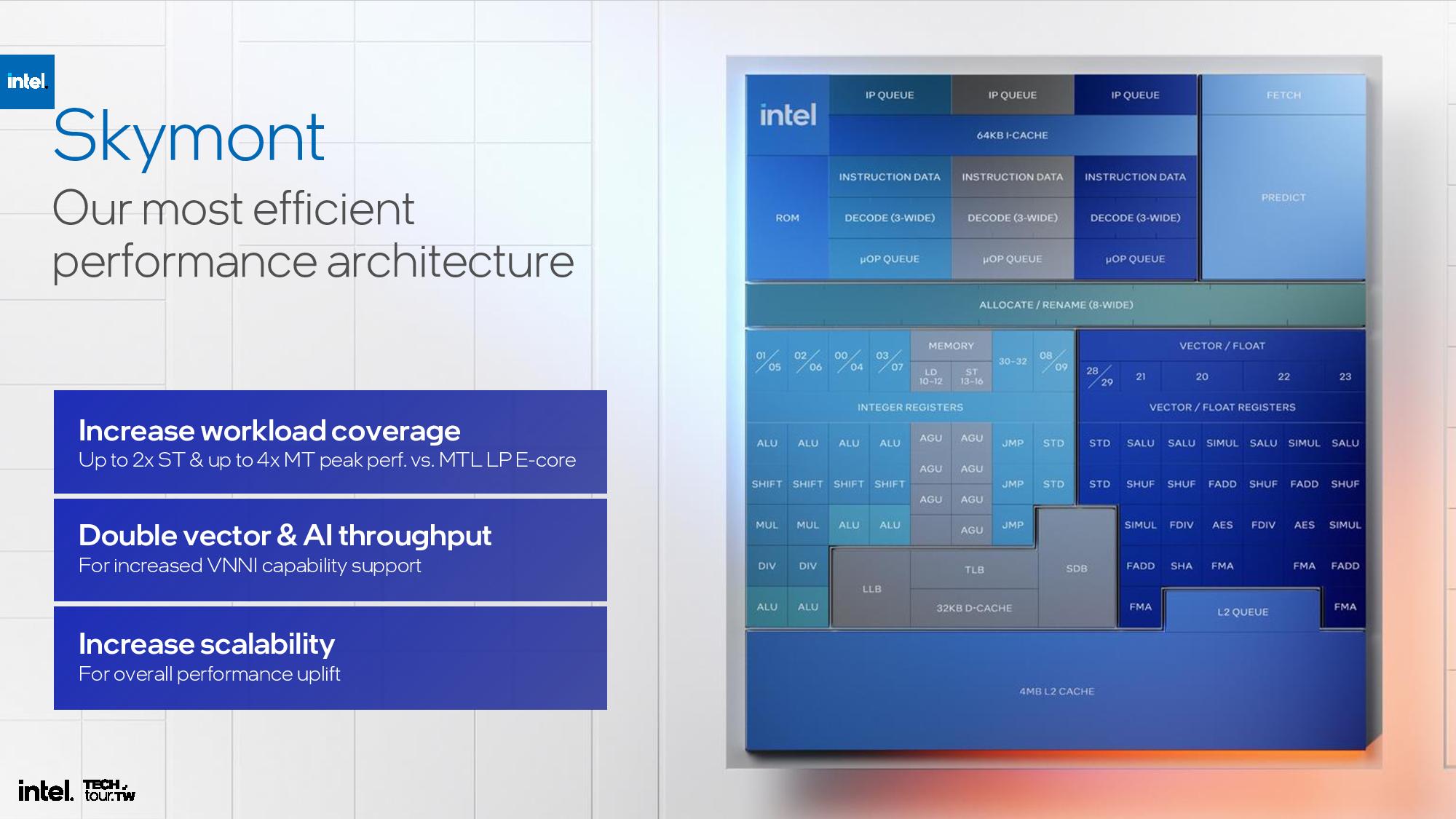
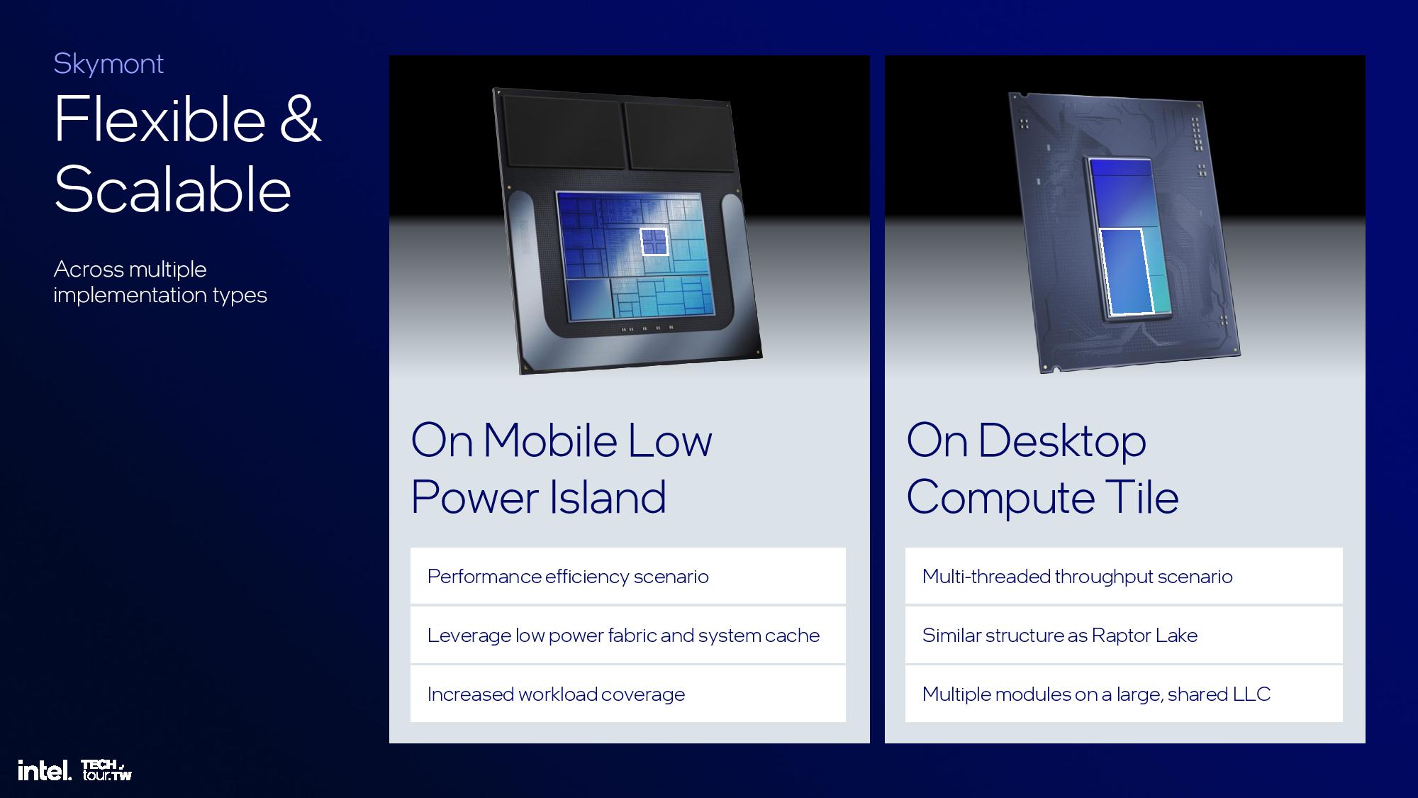
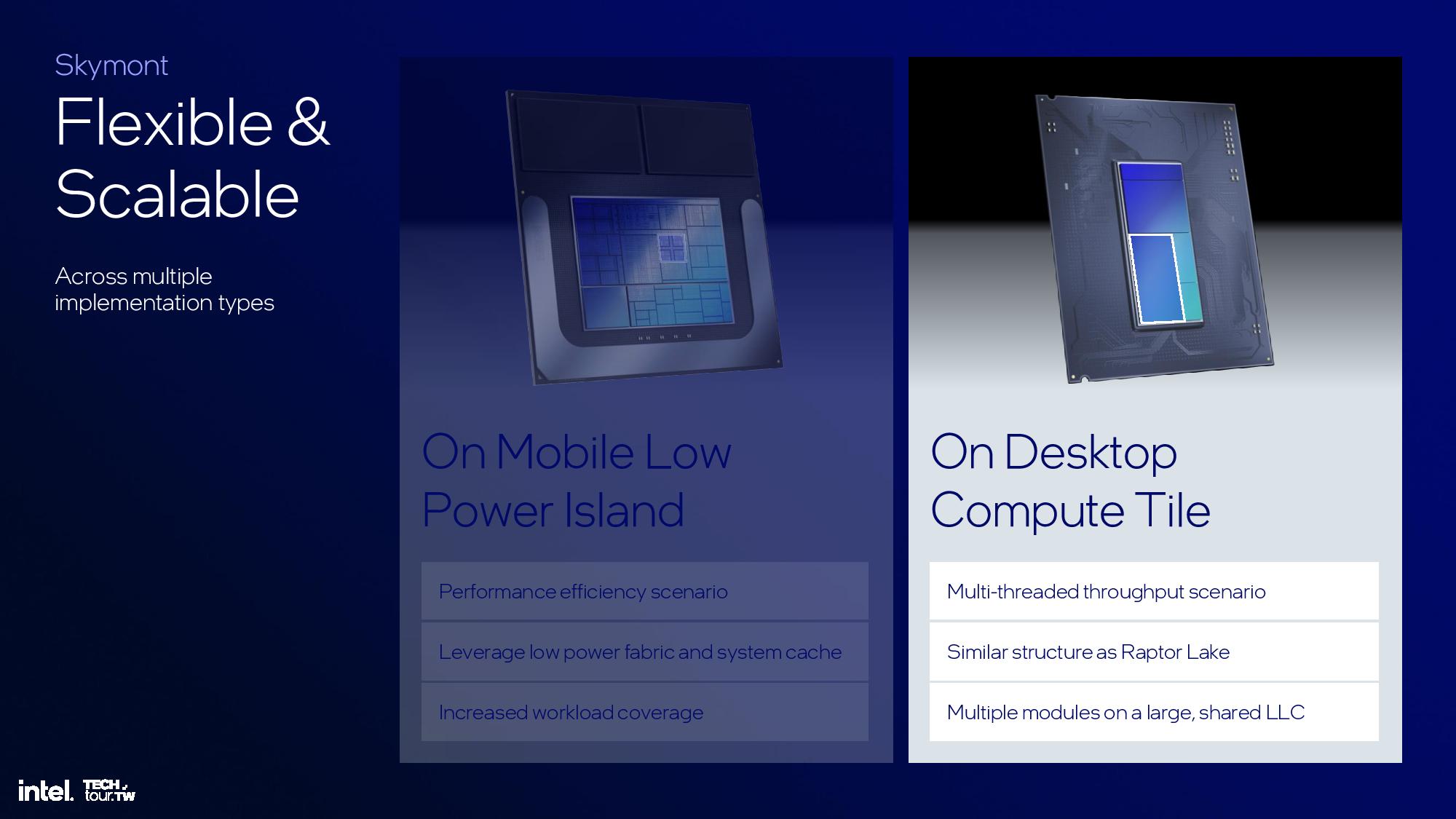
The Skymont architecture marks Intel’s third E-core design for x86 hybrid processors, following Gracemont in Alder Lake and Crestmont in Meteor Lake. (That's not counting the Tremont cores in Lakefield, which seem to be more of a proof of concept in hindsight.) The Meteor Lake design employed two E-cores placed in the SoC tile for extreme low-power workloads, with four additional E-cores on the compute tile along with the P-cores. With Lunar Lake, Intel employs a single quad core cluster on the compute tile to addresses both the low power E-core and high-power E-core roles with an expanded dynamic range.
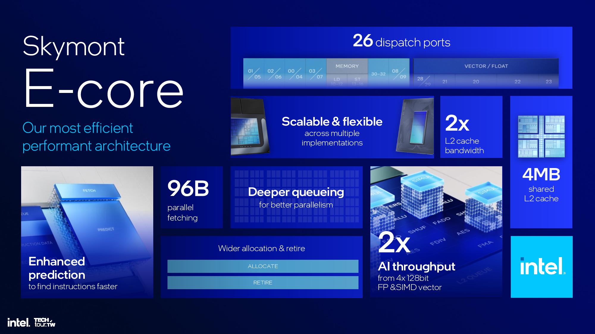
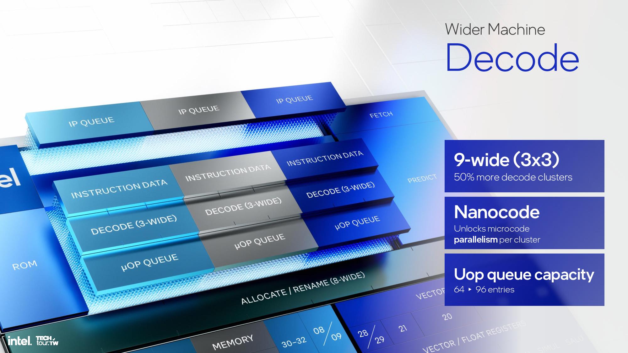
Intel optimized the branch prediction engine by incorporating a 96-instruction byte parallel fetch to feed the decode engine. The decode clusters are also expanded from 6-wide (2x3) with Crestmont to 9-wide (3x3) with Skymont, so any core in the new design can sustain nine instruction decodes per clock. Skymont also now employs nanocode to enable parallel microcode generation to allow the three decode clusters to execute in parallel more frequently. Micro-op capacity was also increased from 64 to 96 entries to add more buffering between the front end and back end.
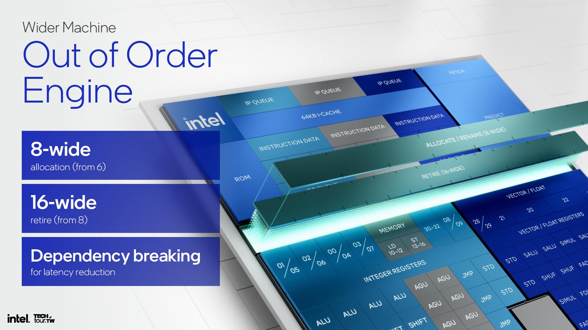
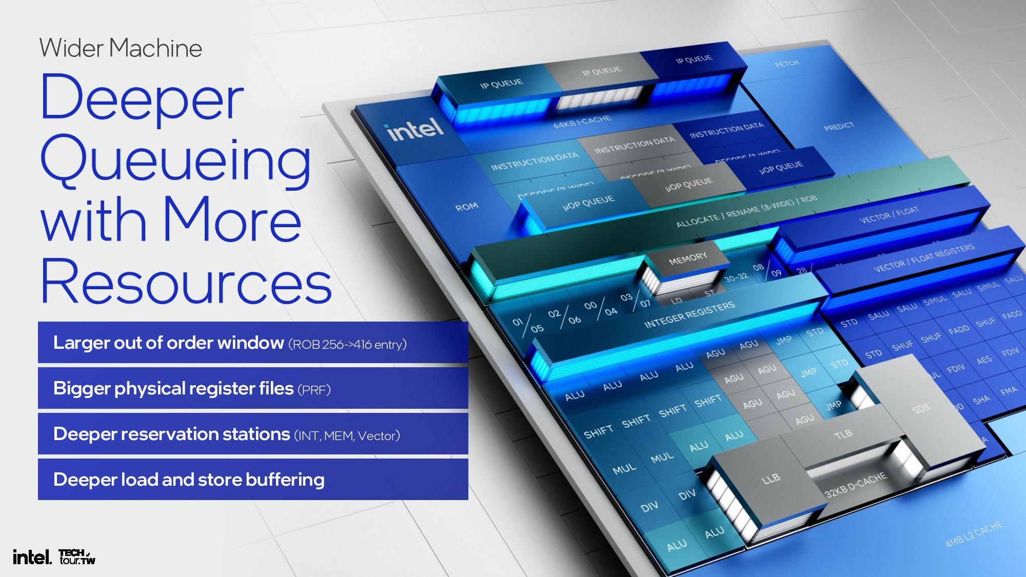
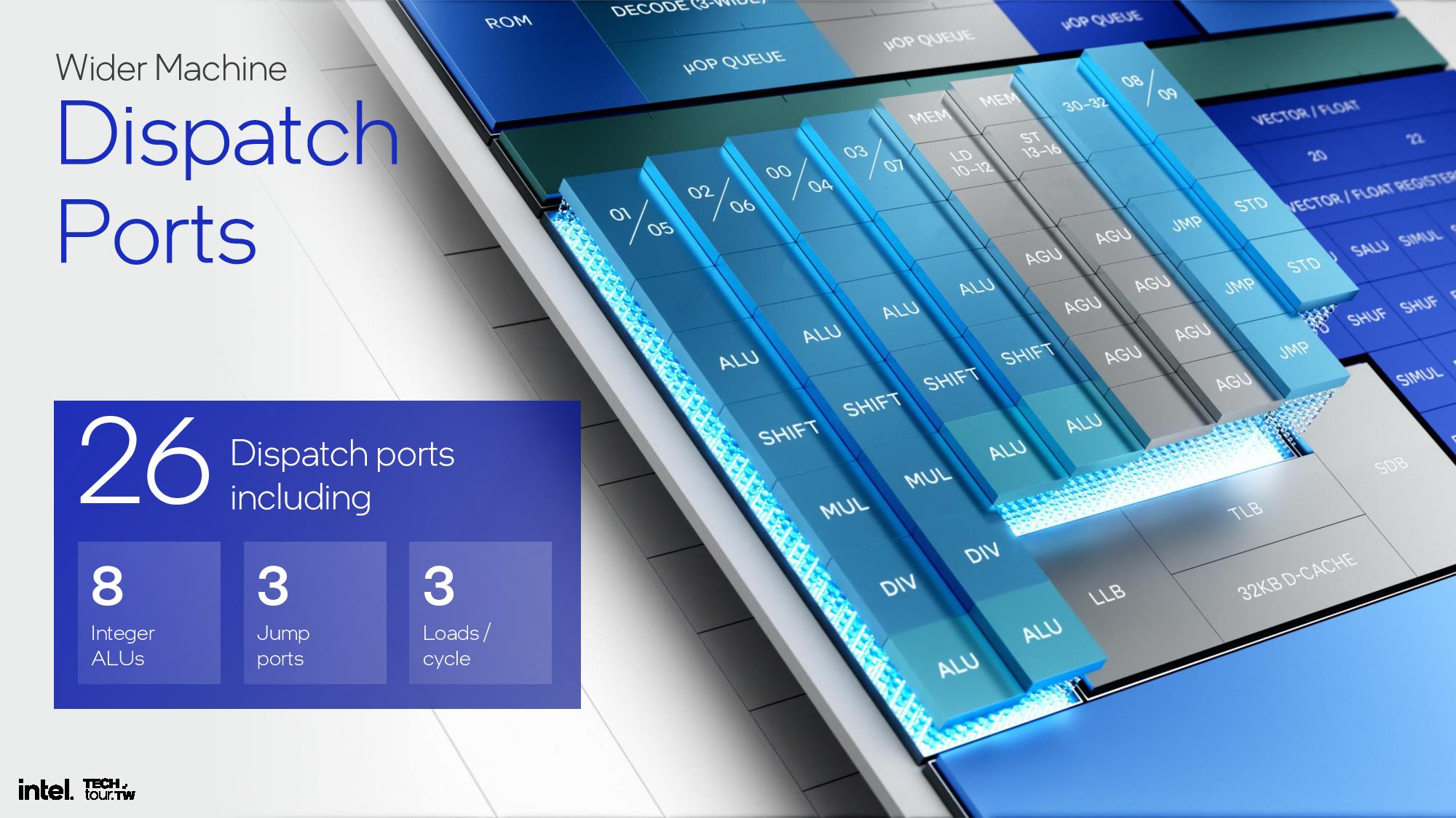
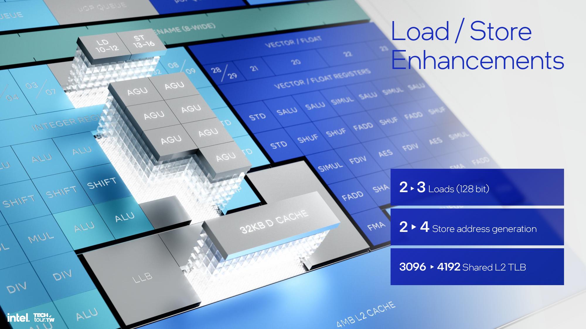
Skymont has an 8-wide allocation in the out of order engine, an increase from Crestmont’s 6-wide allocation. Skymont also expands to a 16-wide retire, a doubling over Crestmont’s 8-wide retire, to free up resources as quickly as possible after stalls, which improves power and area efficiency. The out of order window is 60% larger than the prior-gen, and the architecture has bigger register files, deeper reservation stations, and deeper load and store buffering. Parallelism is boosted by employing 26 dispatch ports, including eight ALUs, three jump ports, and support for three loads/cycle.
Intel targeted a 2X improvement in vector performance, made by going from the two 128-bit FP and SIMD vector pipes to four with Skymont. Other improvements to the vector engine targeted latency reductions and adding support for floating point rounding. Intel also enhanced its load/store engine with a few enhancements listed in the slide.
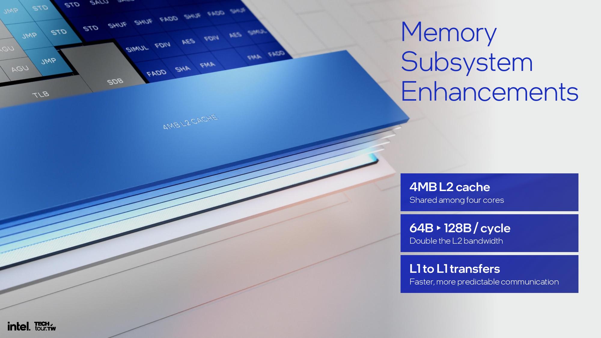
Previous E-core clusters had a shared 2MB L2 cache, but that has now been expanded to 4MB with double the L2 bandwidth. L1 to L1 transfer bandwidth was also improved.
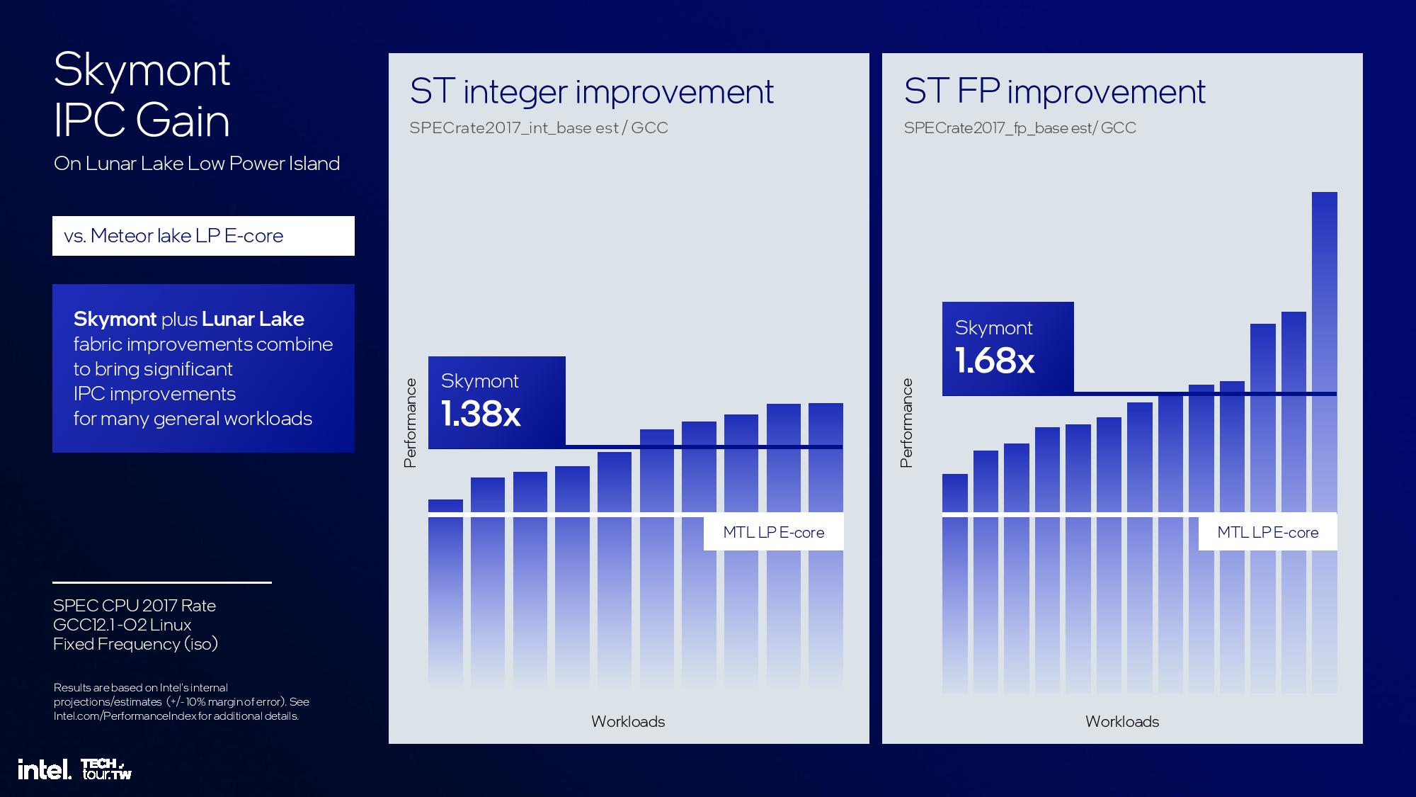
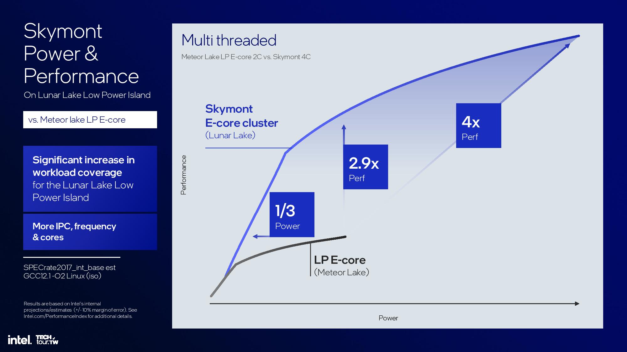
The final results are impressive, with the aforementioned 38% and 68% improvement in single-threaded integer and floating-point performance, though this is notably compared to the low-power e-cores in the Meteor Lake SoC, not the standard quad-core cluster on the compute die. Again, Intel gives itself a rather large +/- 10% margin of error.
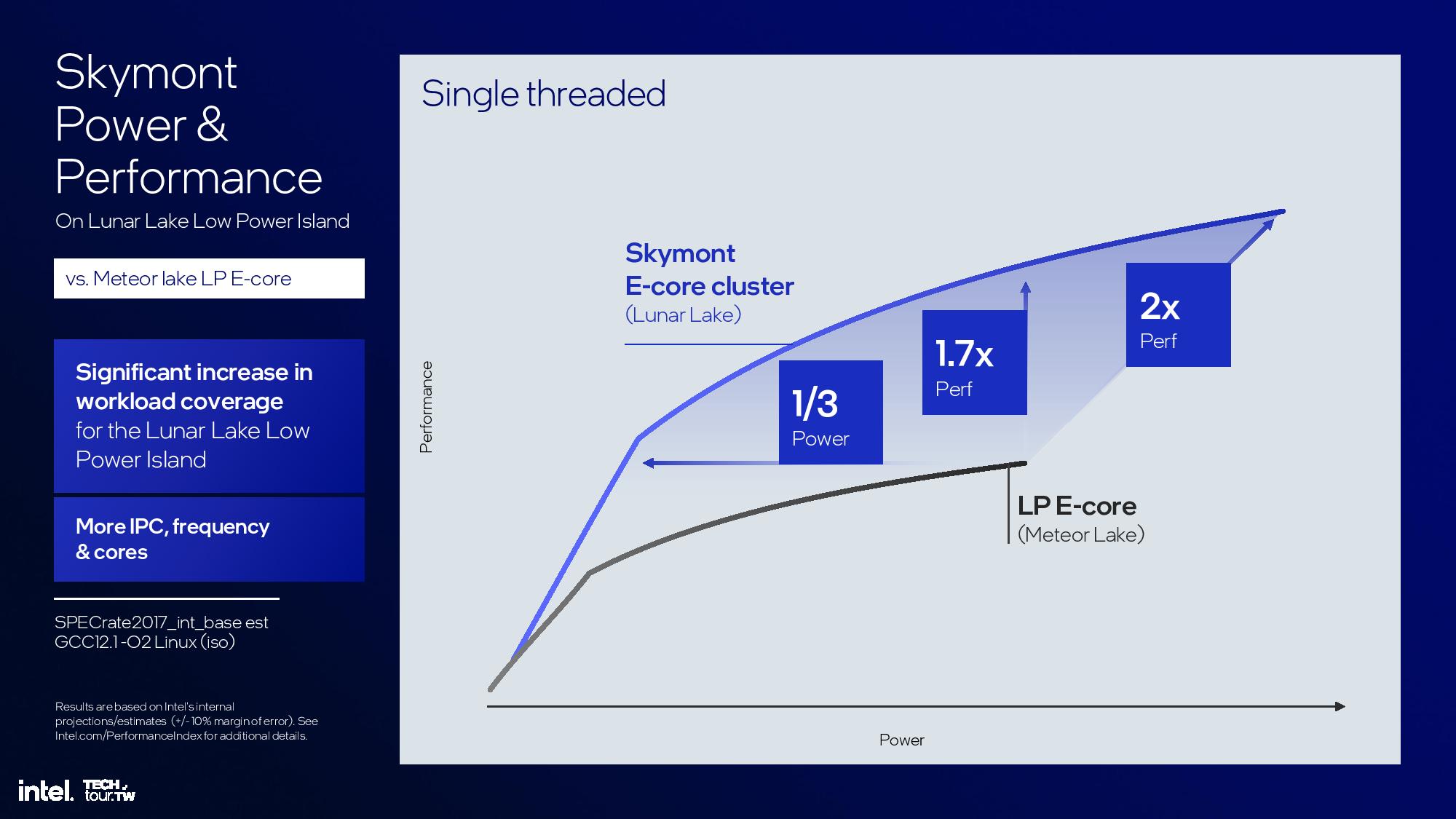
Skymont’s power and single-threaded performance curve is vastly enhanced over Crestmont, but the comparisons are once again being made to the low-power Meteor Lake E-core instead of the full E-core. Compared to Crestmont’s peak performance, Skymont consumes one-third the power to deliver the same level of performance. However, it has more gas in the tank with 1.7X more performance at the same power level. Overall, Skymont’s peak single-threaded performance is twice that of the Crestmont LP E-cores.
The multi-threaded power/performance metrics are skewed, as Intel compares Skymont’s quad-core cluster to Meteor Lake’s dual-core low-power E-core cluster instead of comparing it to the quad-core cluster. As such, we would expect to see half the stated advantages in these areas over the standard Meteor Lake quad-core cluster.
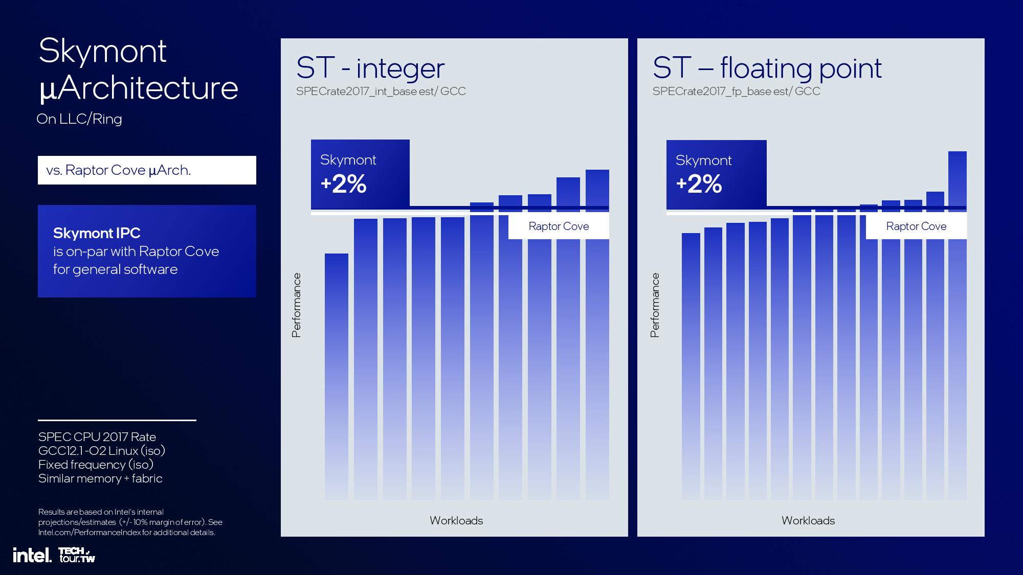
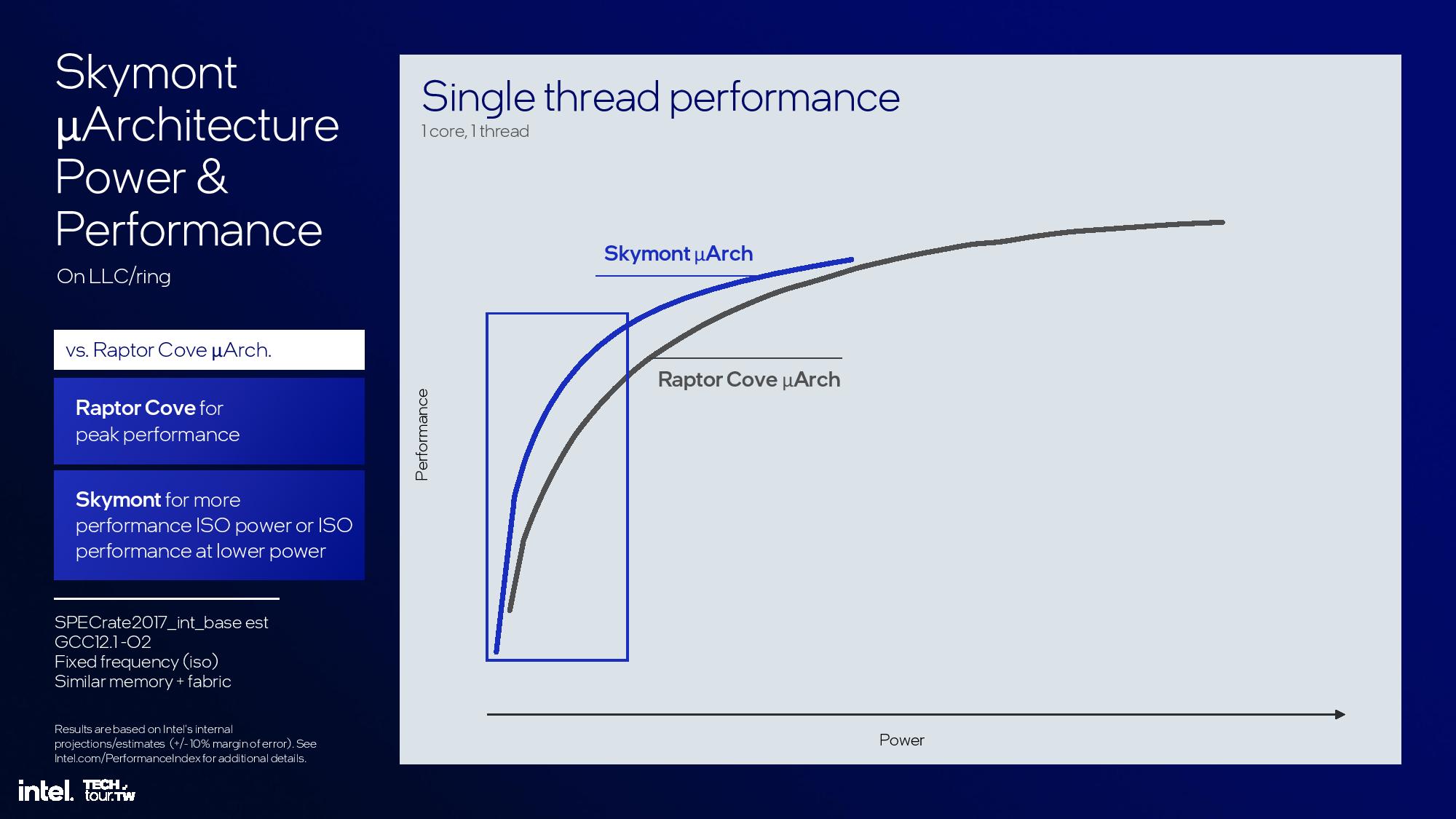
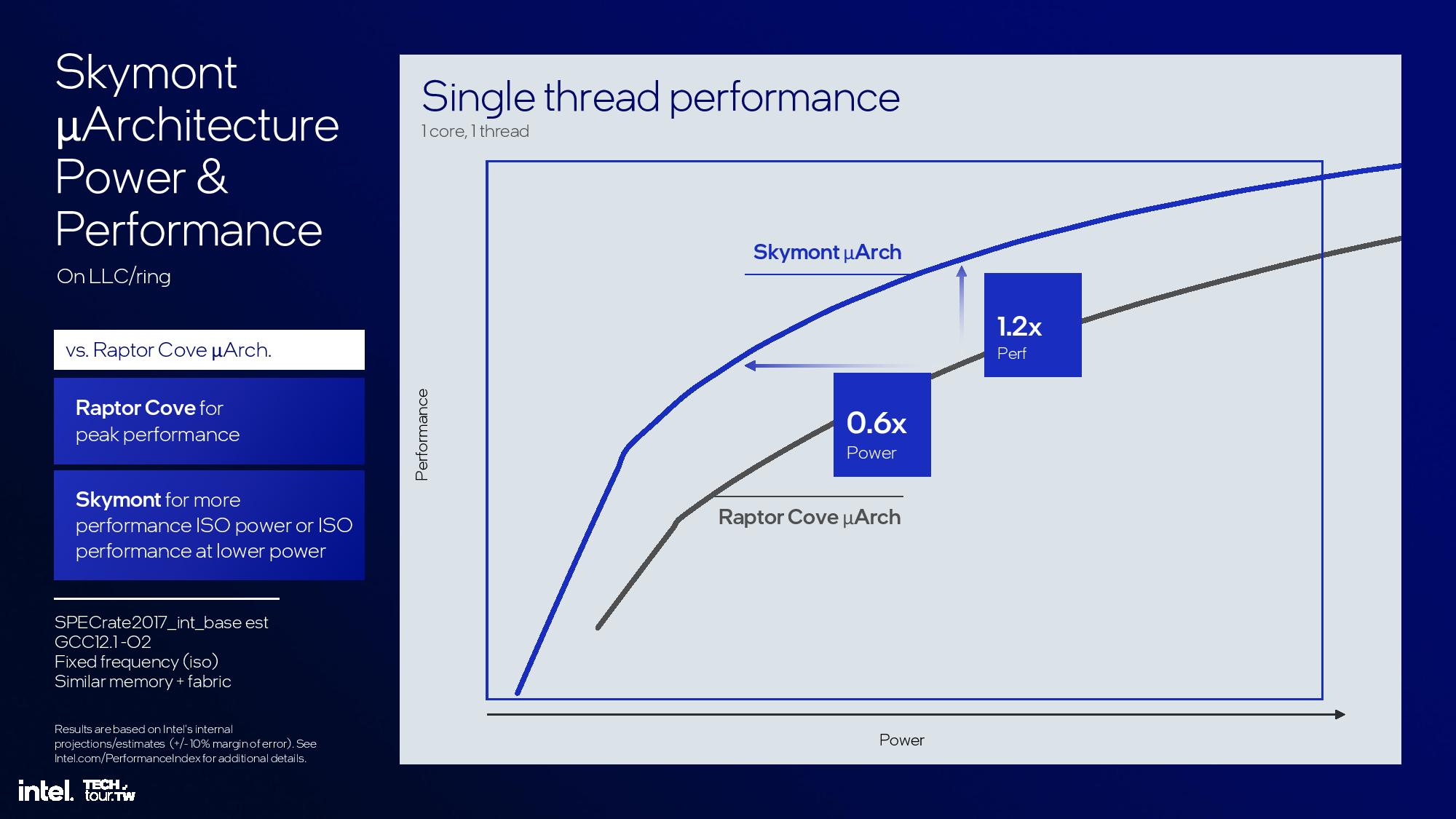
Intel also provided comparisons for Skymont vs Raptor Lake’s P-core, which uses the Raptor Cove architecture. Intel claims a 2% advantage for Skymont in integer and floating point.
Intel’s power-to-performance slides for the Skymont/Raptor Cove comparisons are easily misconstrued. In the last two slides, we can see that Intel zoomed in on an area of the power/performance curve that it says is the proper power envelope for multi-threaded acceleration on a low power island. That yields the final slide, where Intel says that Skymont consumes 0.6X the power at the same performance as Raptor Cove, or 1.2X the performance at the same power. Again, we see the same high margin of error, so take these extrapolated comparisons with a healthy serving of salt.
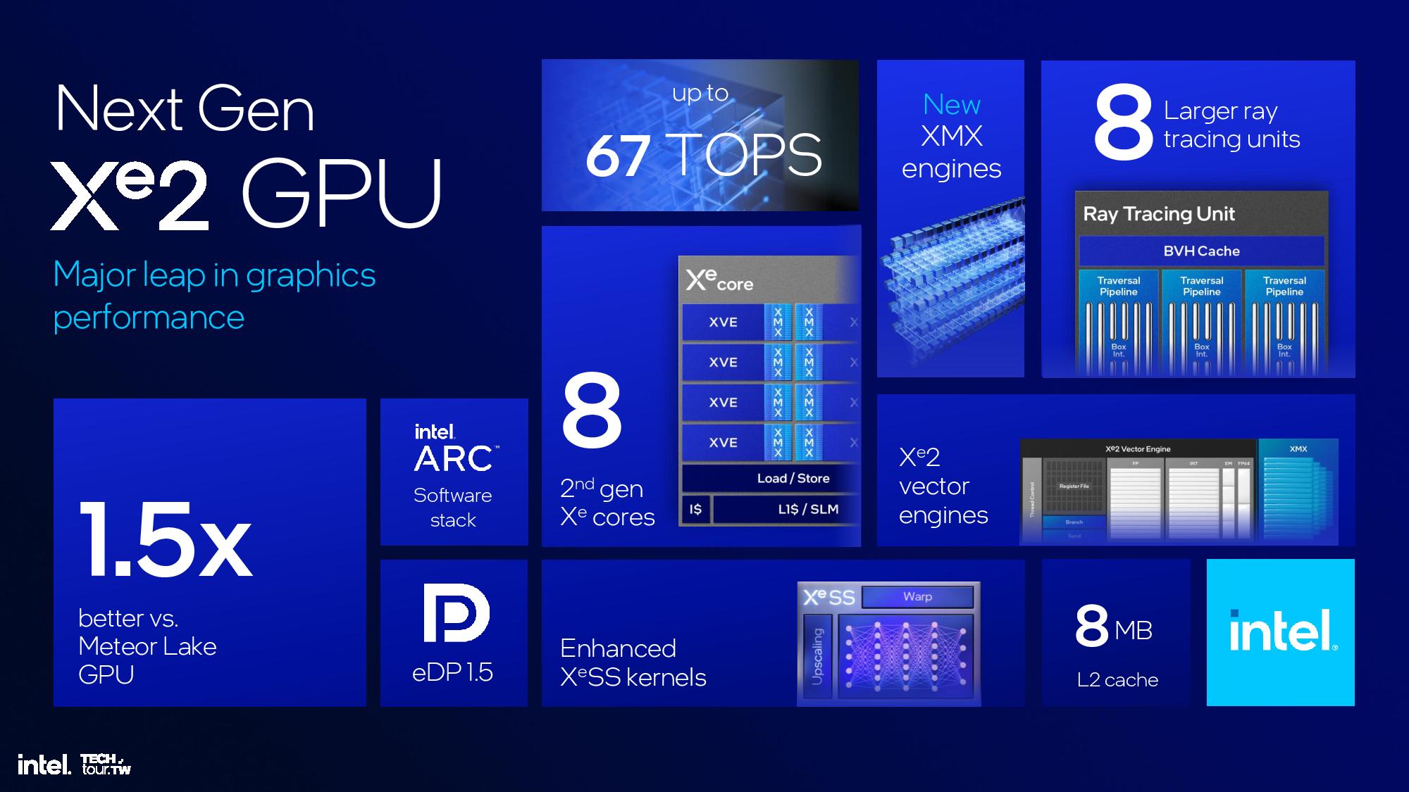
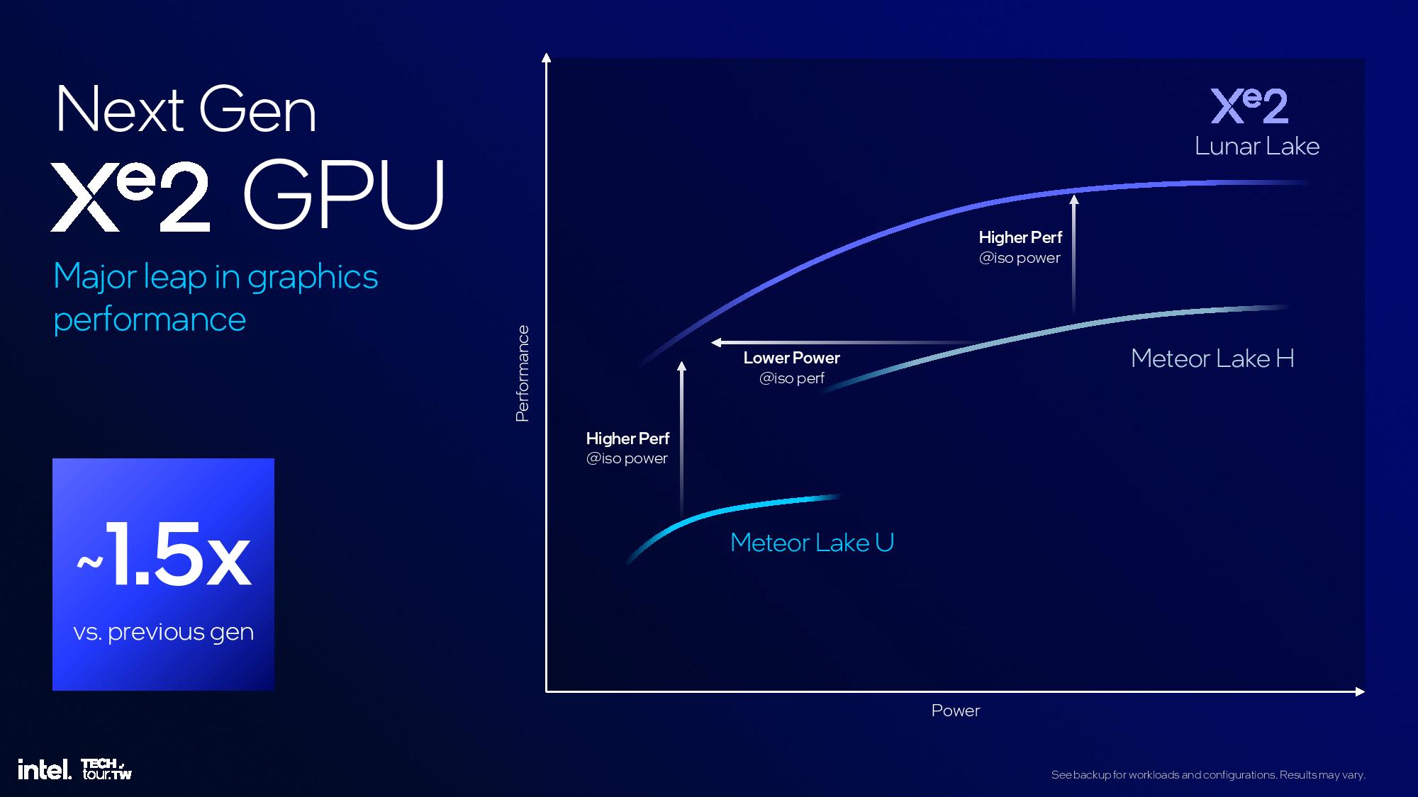
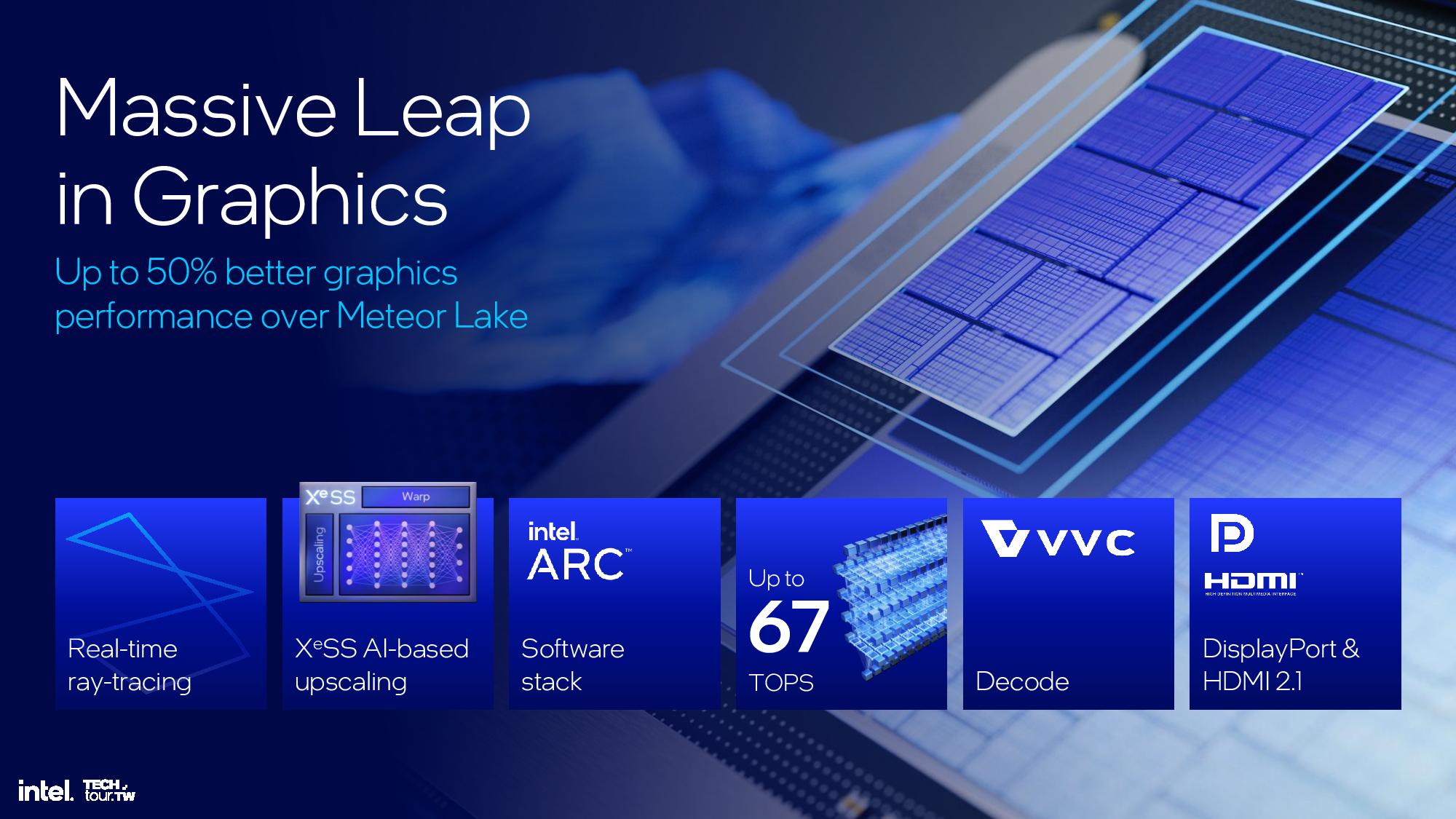
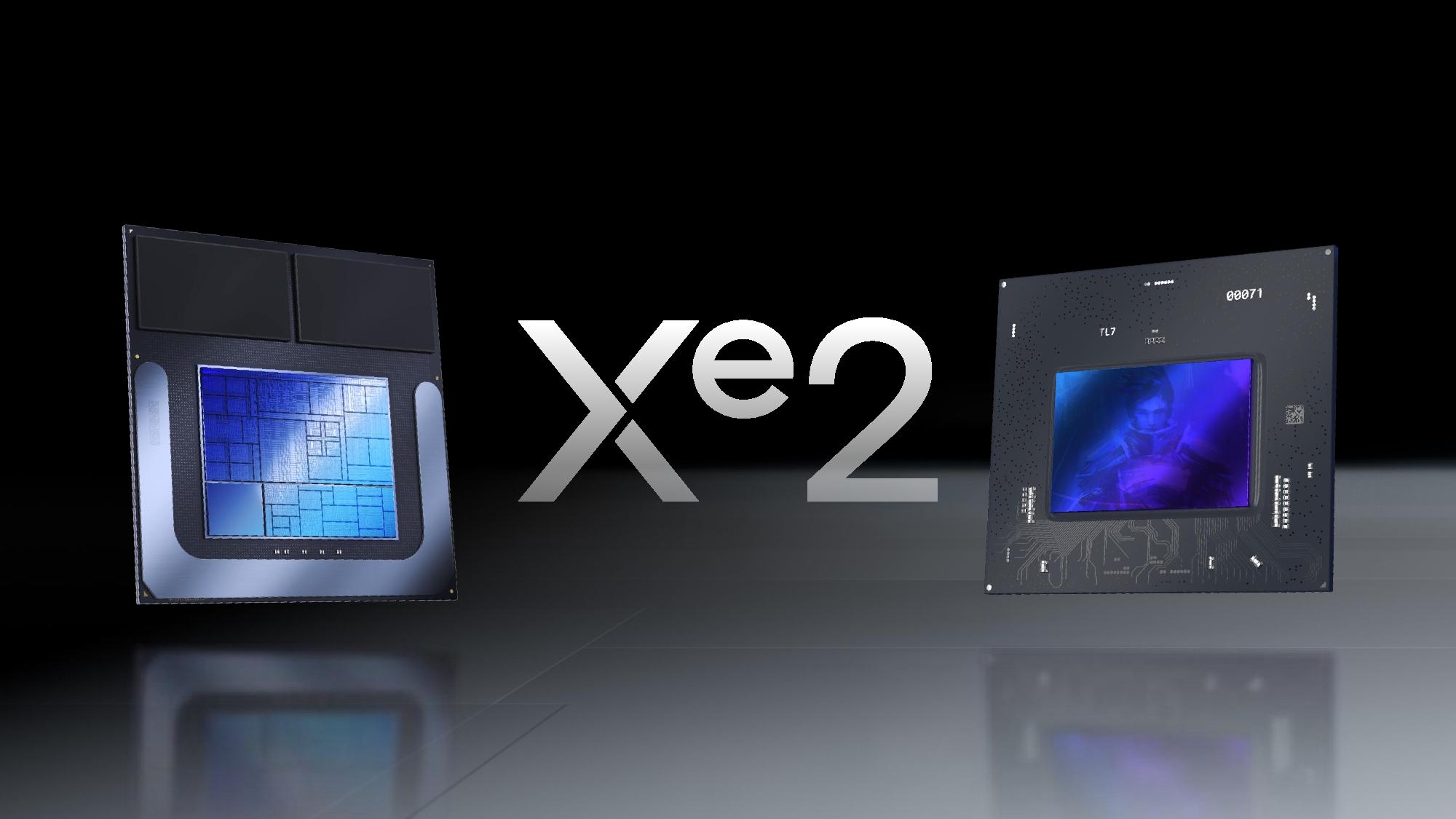
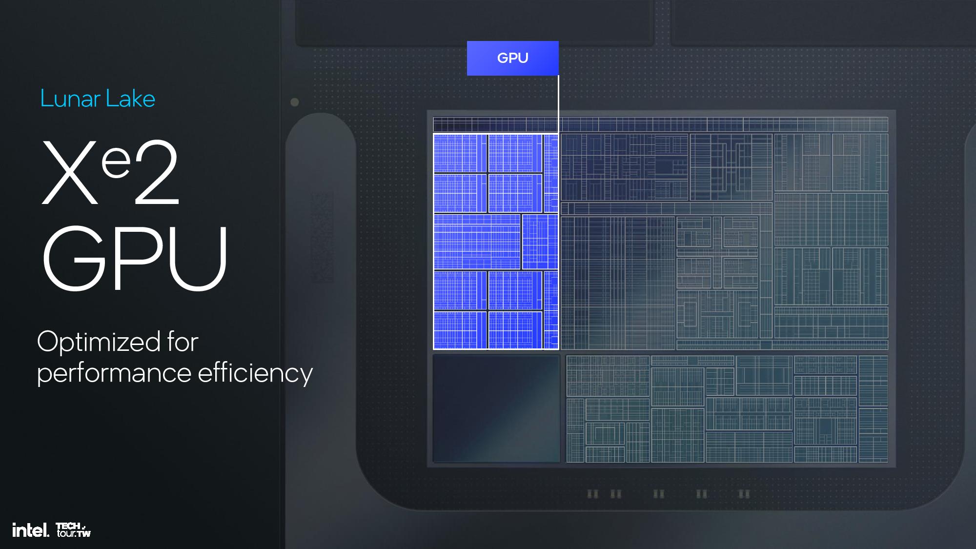
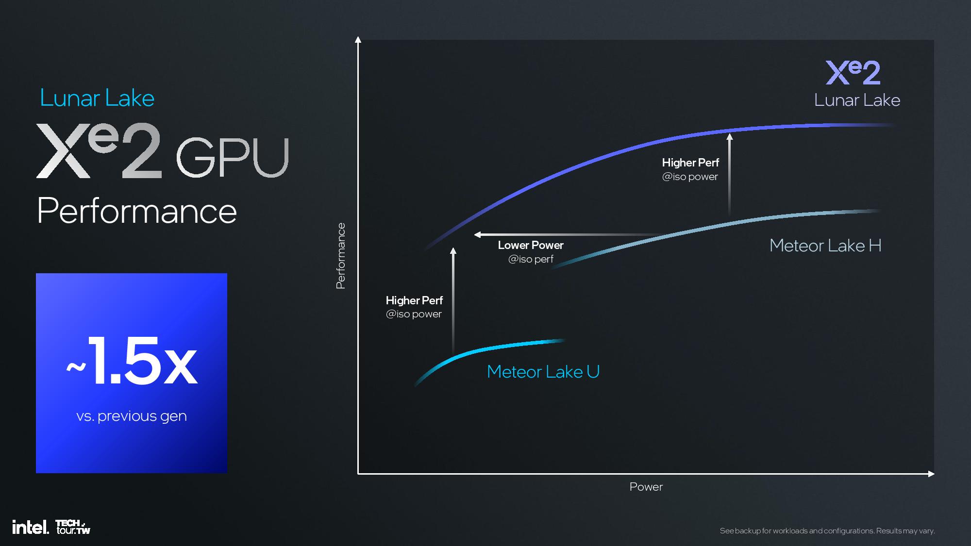
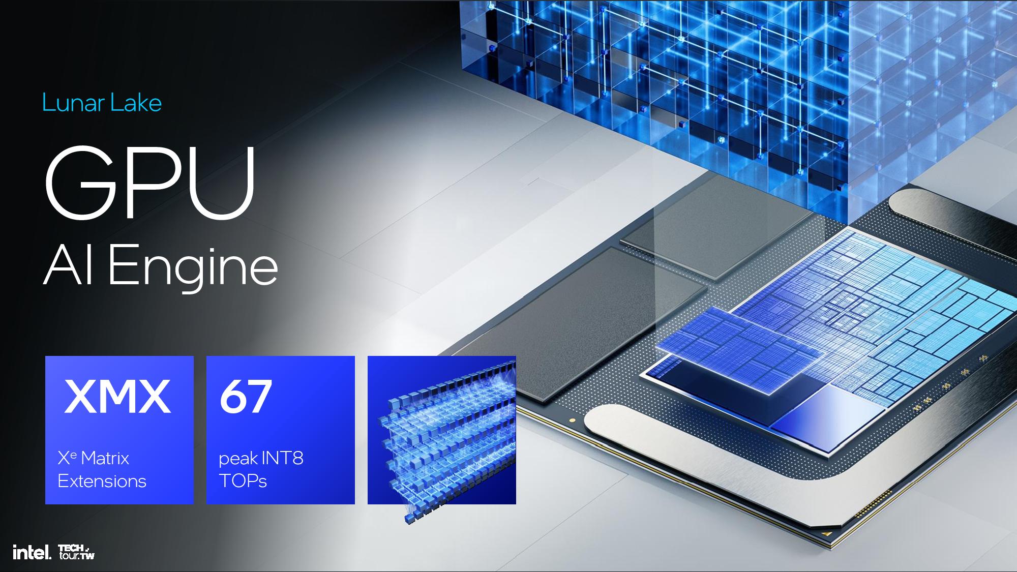
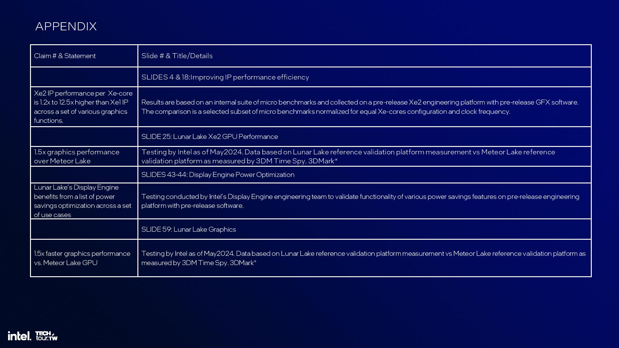
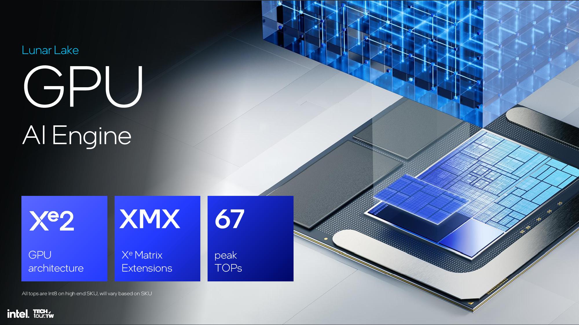
The new Xe2 iGPU delivers up to 1.5X more graphics performance than Meteor Lake's Arc Graphics, with up to 67 TOPS of AI performance. Intel has also simplified the naming of its GPU architecture and will simply refer to it as Xe2 in all configurations, as opposed to the Xe-LP, Xe-HP, and Xe-HPG suffixes used with the prior-gen Xe architecture.
Intel’s Xe2 architecture will not only come in the Lunar Lake processors, but it will also be used in the upcoming Battlemage discreet gaming GPUs. However, while the architecture may be the same, Lunar Lake uses lower-power transistors while Battlemage will employ faster transistors to maximize performance. That means the Lunar Lake performance projections can’t be directly extrapolated to predict the performance of Battlemage GPUs — not to mention dedicated GPUs will have dedicated VRAM as well.

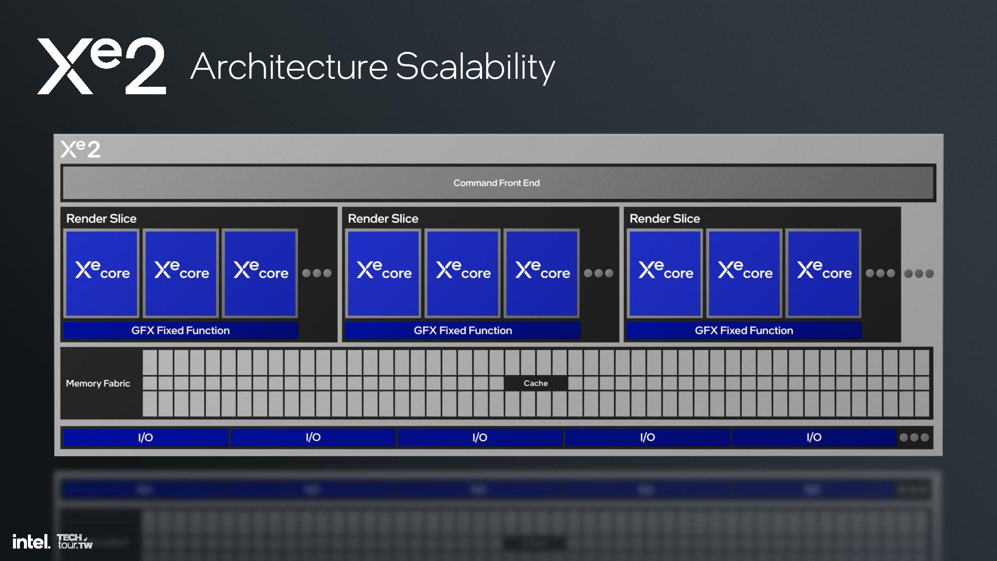
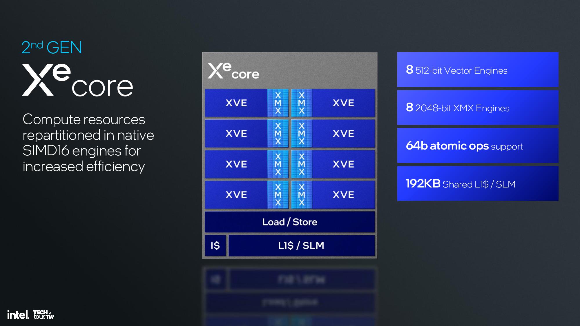
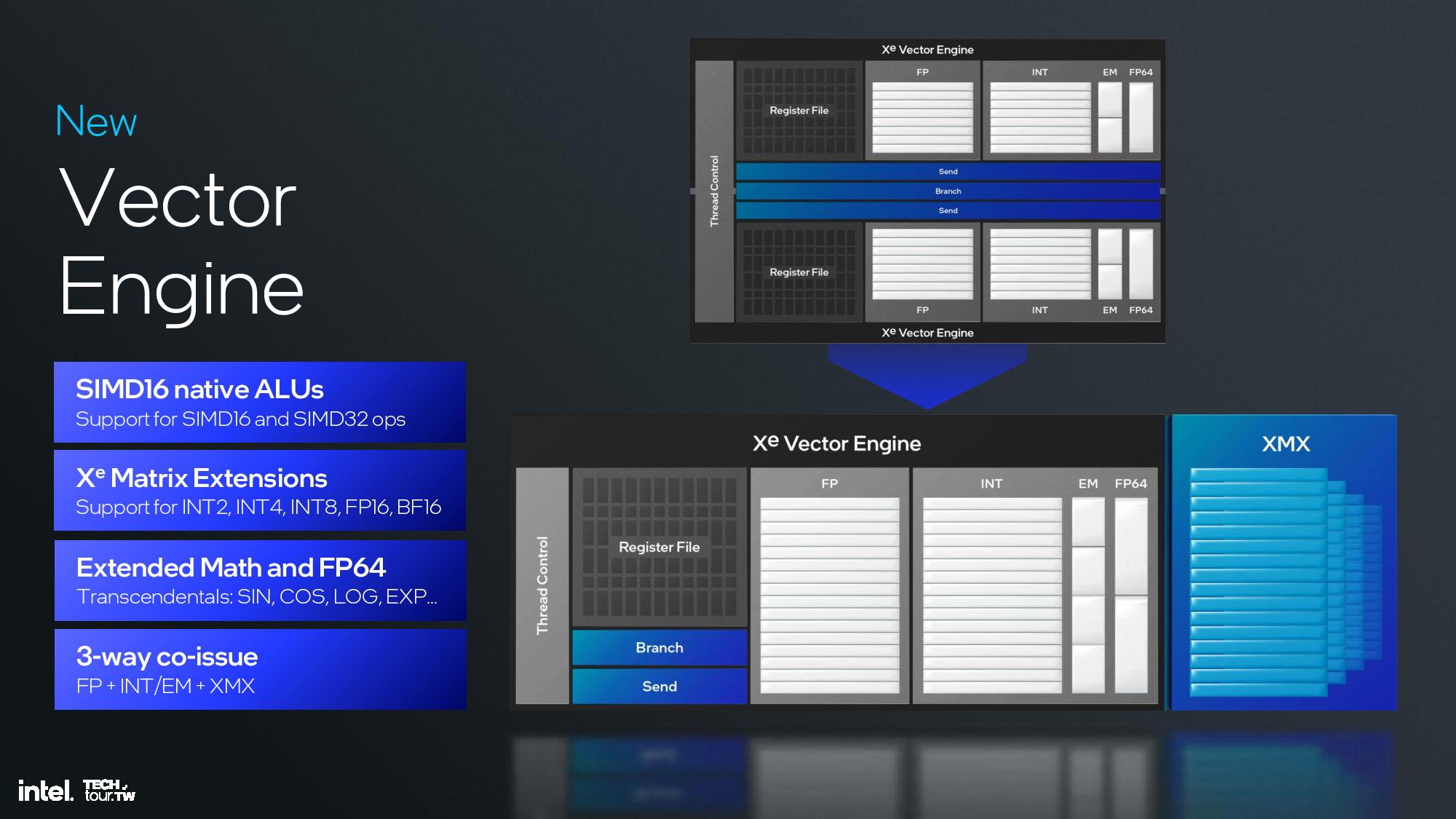
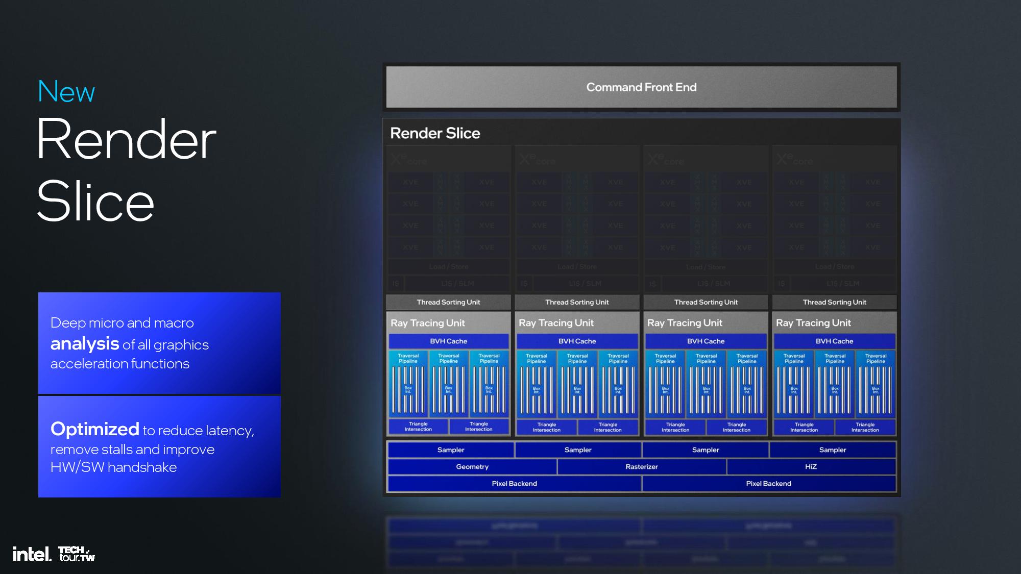
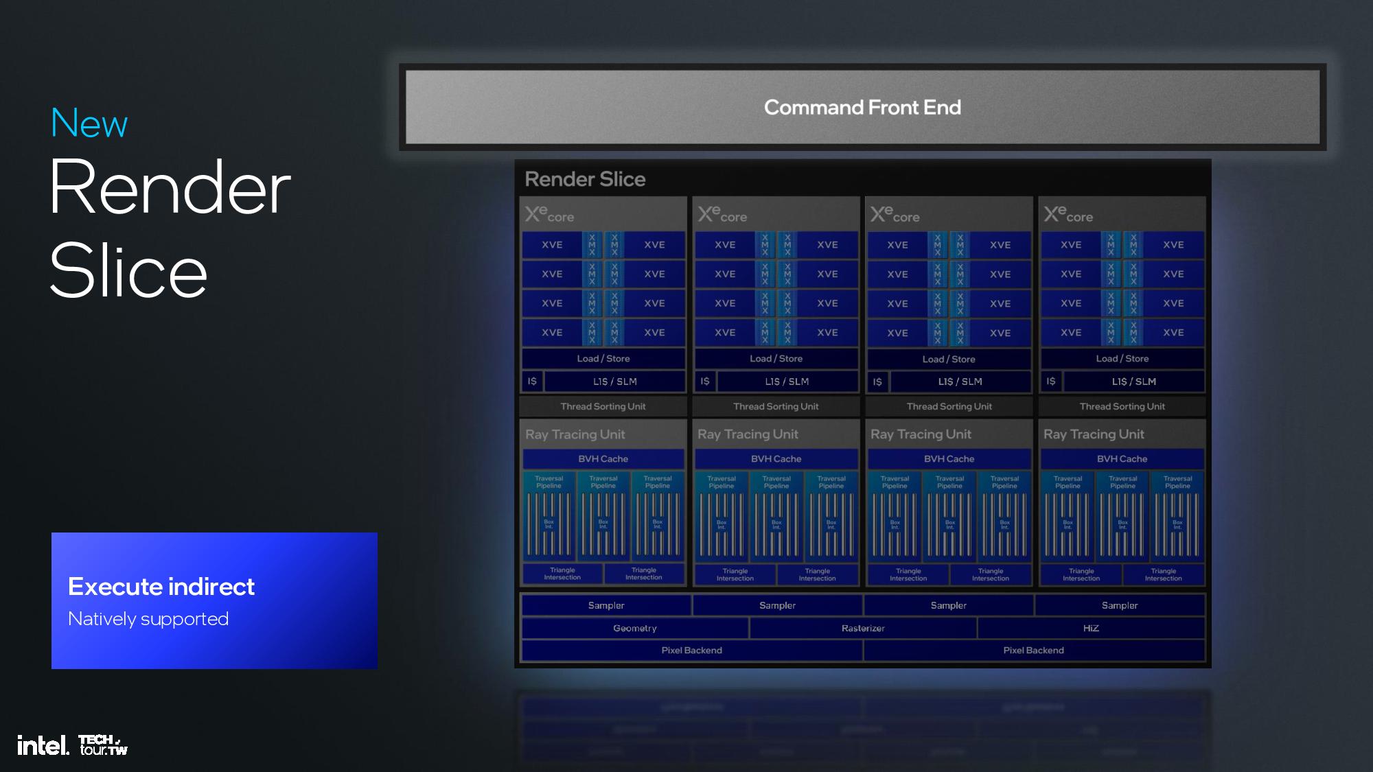
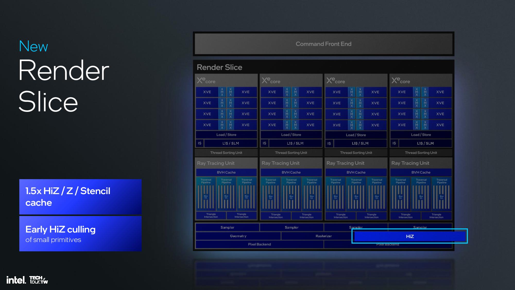
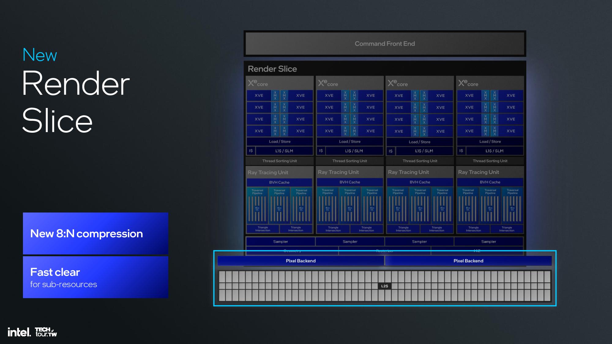
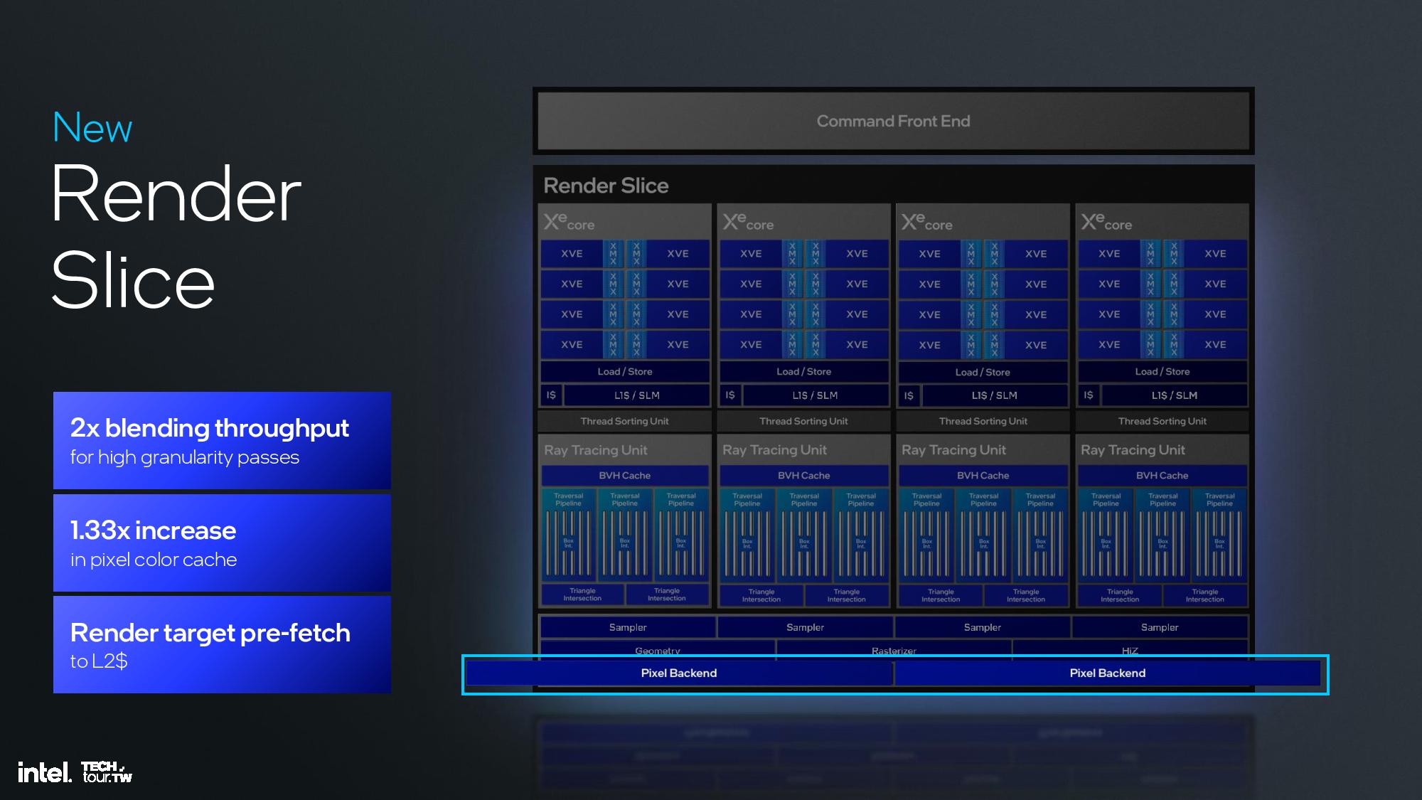
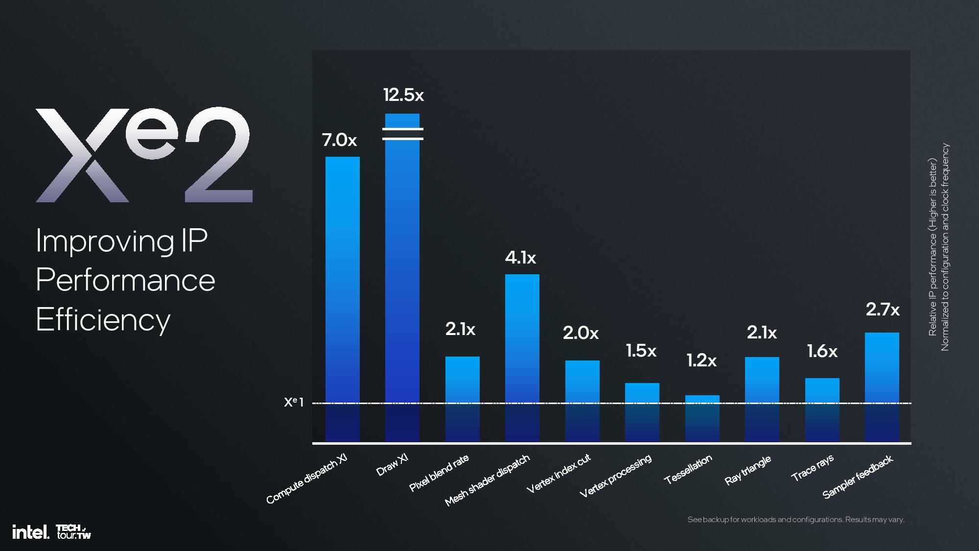
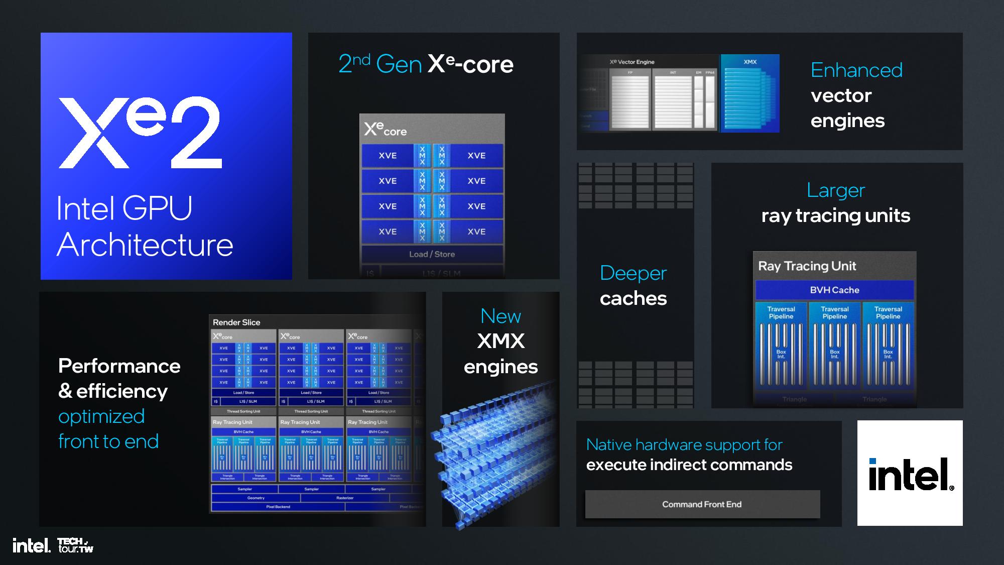
The Xe2 GPU architecture features Intel's second-gen Xe core, larger XMX engines that support more data types, enhanced vector engines, larger ray tracing units, and deeper caches. The GPU is broken down into second-generation Xe cores and render slices, along with fixed functions graphics hardware for tasks like geometry processing, texture sampling, and rasterization. These units are connected to a large cache and memory fabric, along with I/O accommodations that vary based upon the implementation. The design is inherently modular, so it can be easily scaled to either more or fewer units.
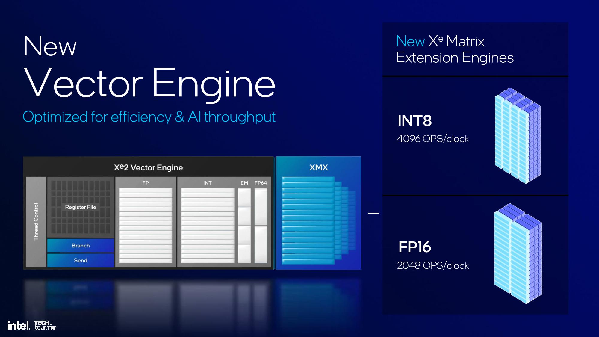
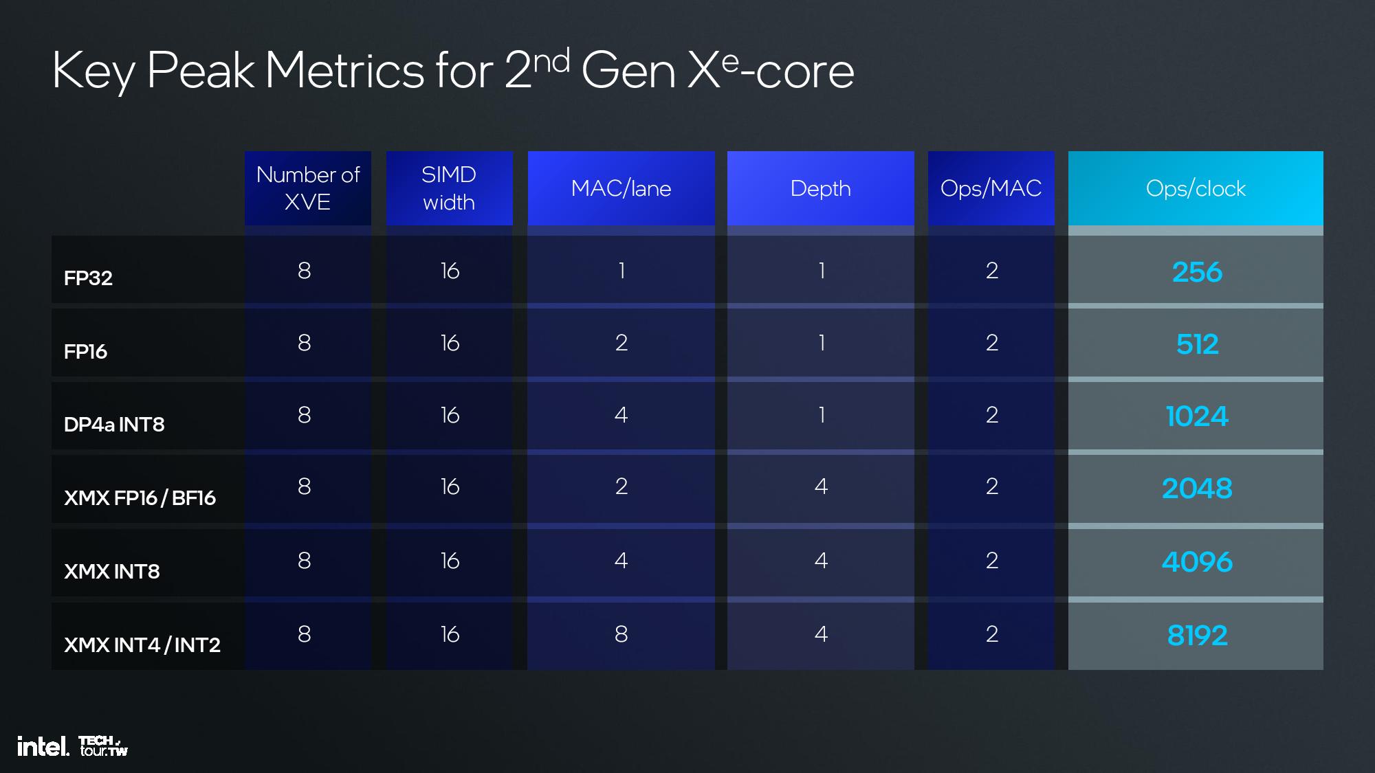
The second-gen Xe core can do eight 512-bit multiplies per clock in the XVE vector engines and eight 2048-bit vectors per clock in the XMX engines. Intel also increased the SIMD engine from 8 lanes wide to 16 lanes wide, which is a more common arrangement that will enhance compatibility. The core also has a 192KB shared L1.
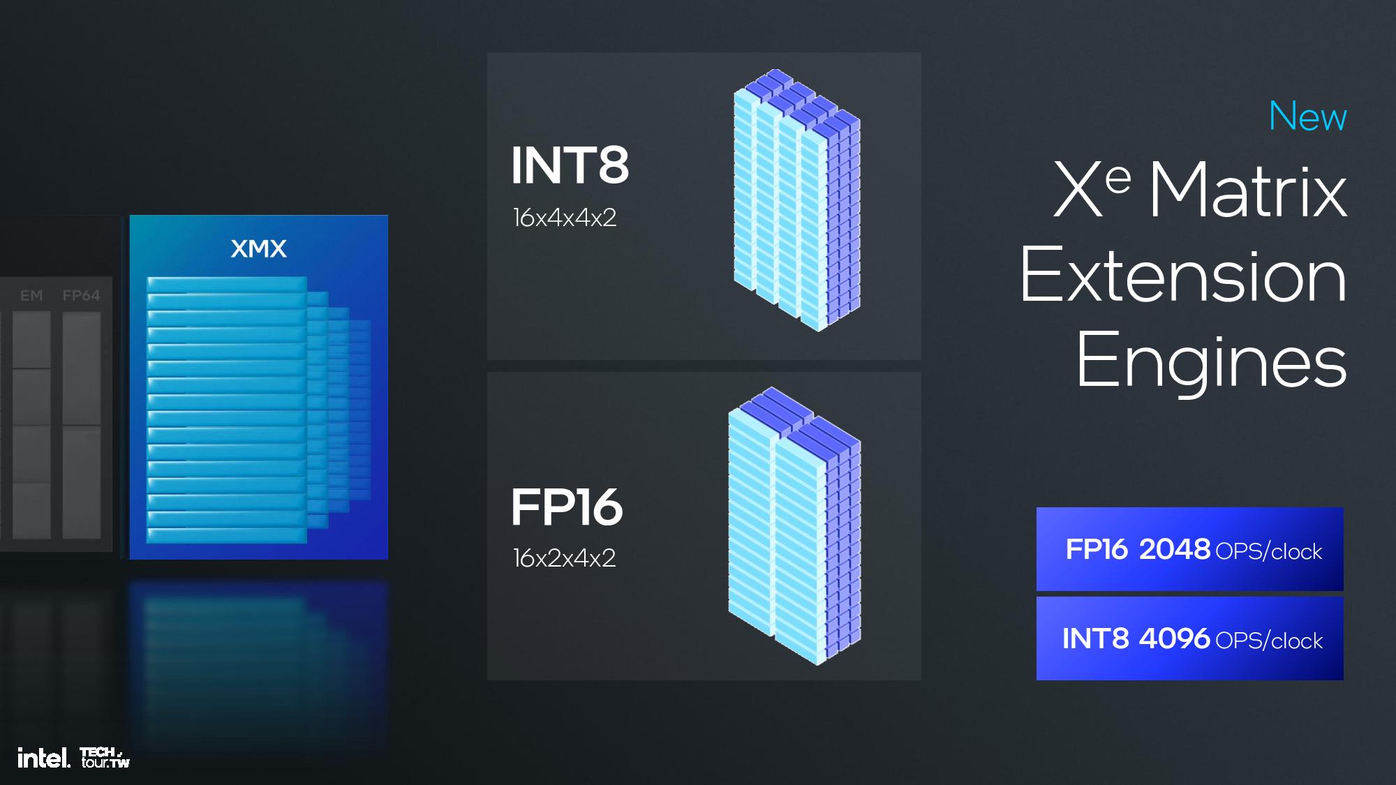
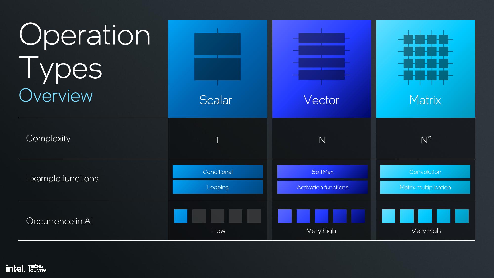
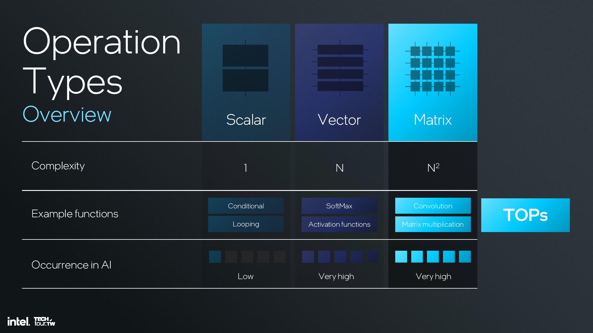
The second-generation vector engine supports INT2, INT4, INT8, FP16 and BF16 for AI operations. You can also see a table that has the calculations for peak TOPS (Ops/clock) in the album above. Note that the previous Meteor Lake iGPU cut the XMX Engine from the design in order to reduce die area and power requirements, so laptops with Xe2 will see significant improvements in AI workloads included XeSS.
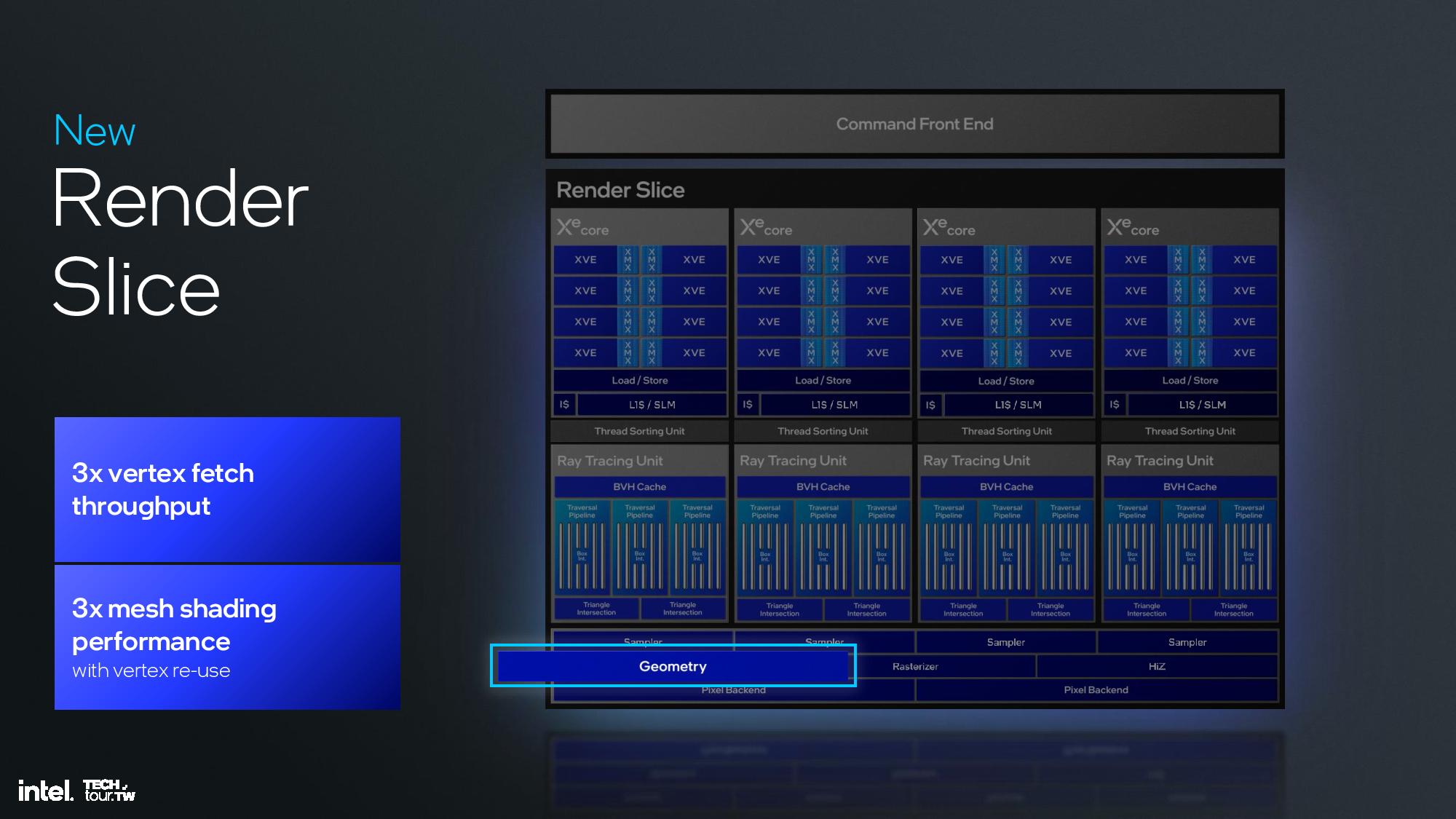
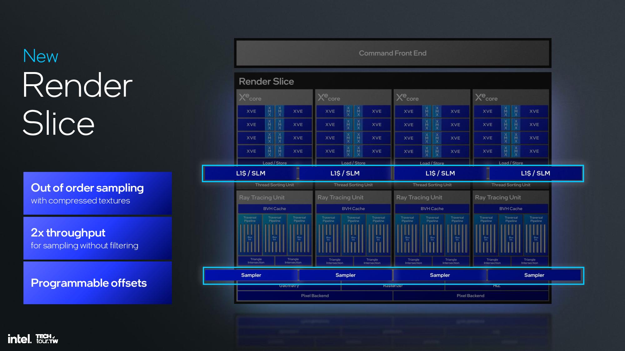
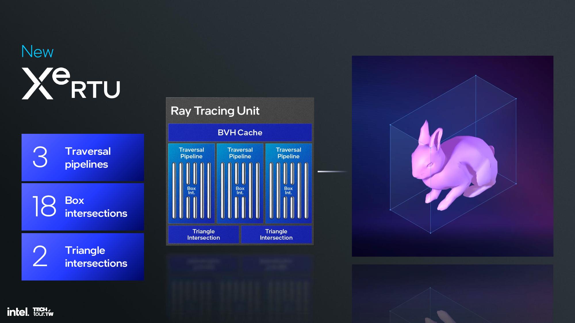
The render slice has also seen plenty of improvements, including a 3X vertex fetch throughput improvement by changing the vertices distribution across the pipeline, a tripling of mesh shading performance via vertex re-use, new support for out of order sampling, and twice the throughput for sampling without filtering, among other improvements. Intel also cites increased ray tracing performance due a reorganized pipeline in the new Xe Ray Tracing Unit (RTU).
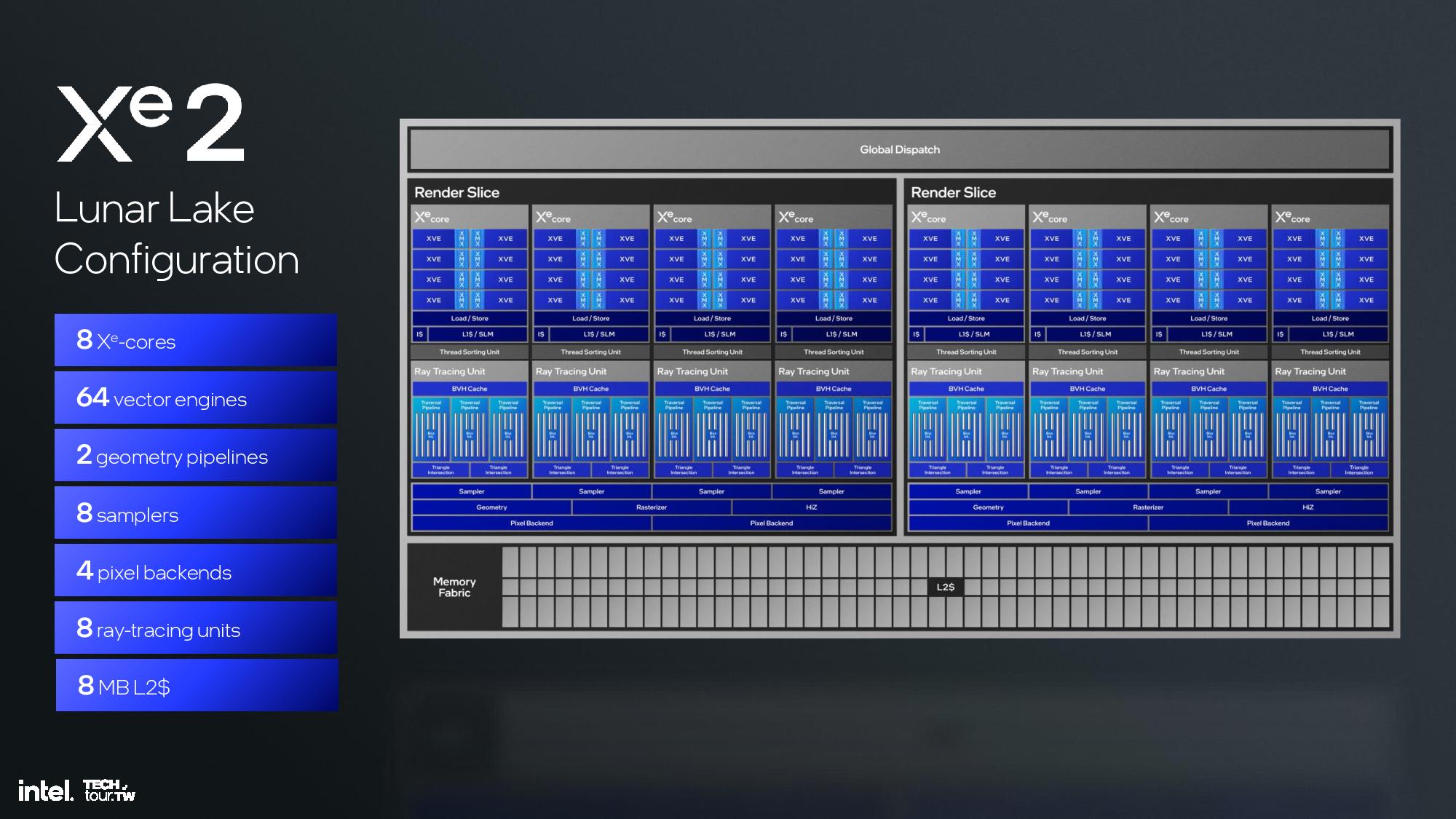

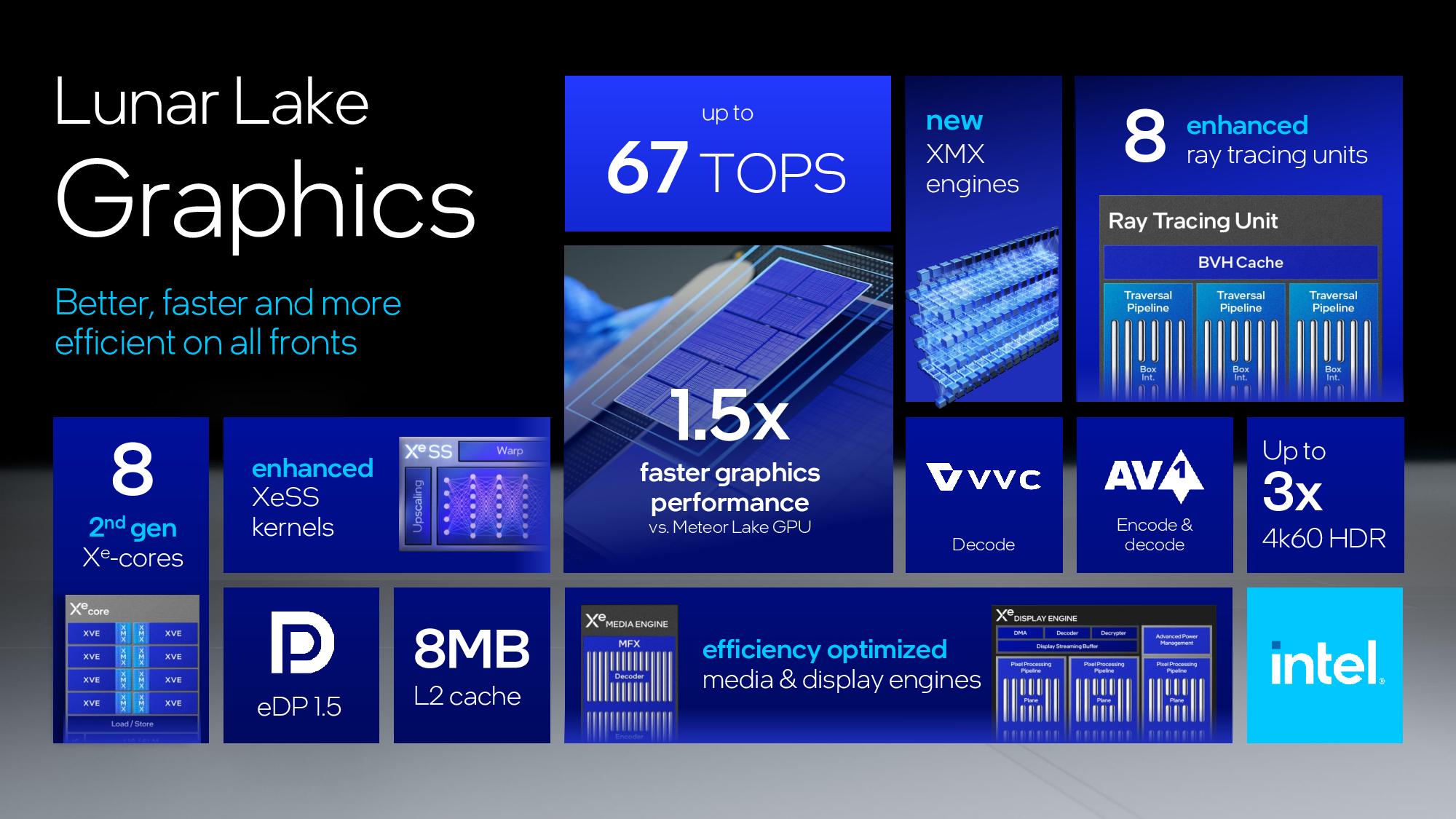
These ingredients are used to create Lunar Lake’s specific iGPU hardware configuration. Lunar Lake comes armed with eight second-gen Xe cores, 64 vector engines, two geometry pipelines, eight ray-tracing units, and 8MB of L2 cache, among other ingredients.
Intel says the Lunar Lake iGPU delivers 1.5X more performance than Meteor Lake-U at the same power threshold. Moving to Meteor Lake-H, Lunar delivers “similarly higher” performance at the upper end of the power range. However, the Lunar Lake GPU is designed for performance-per-watt with lower power transistors.
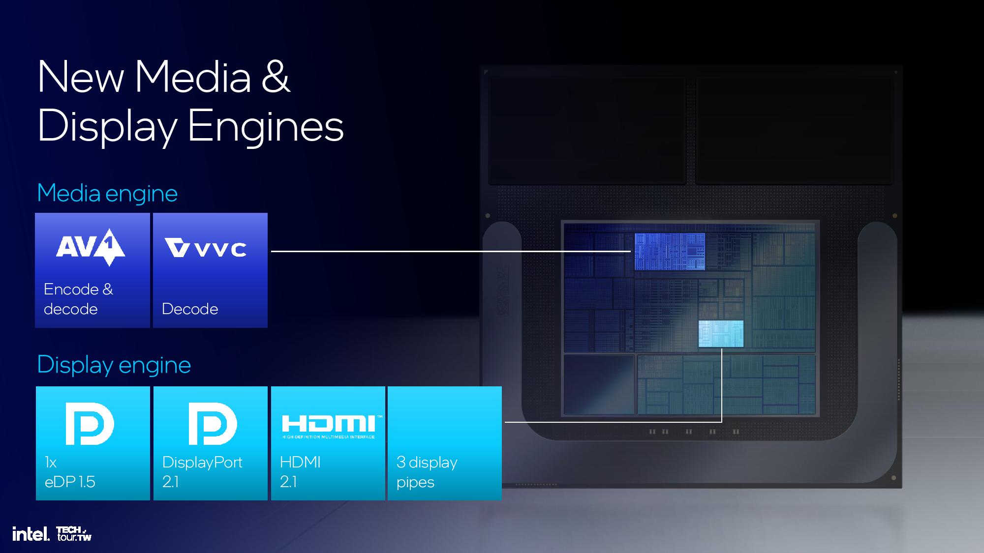
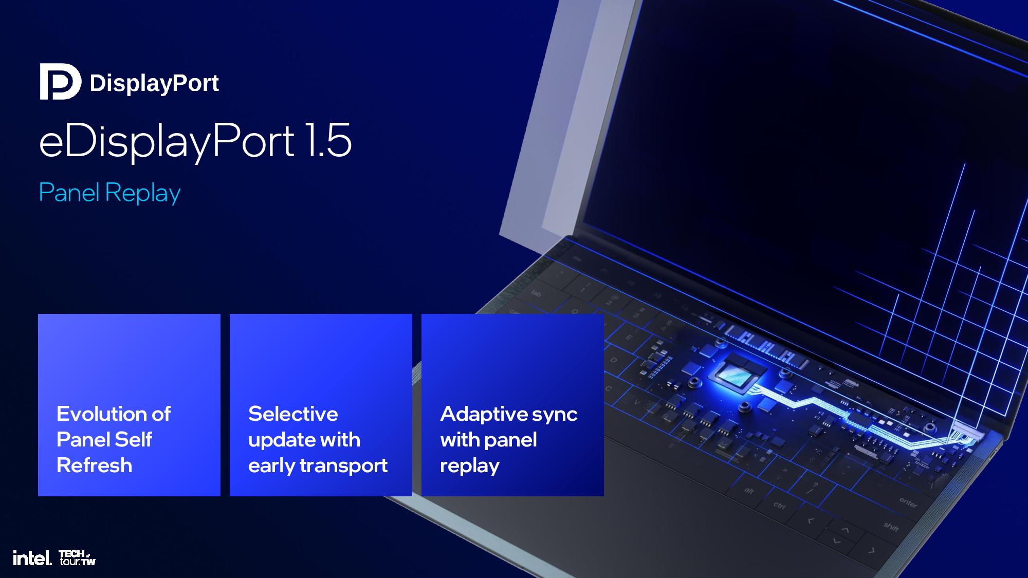
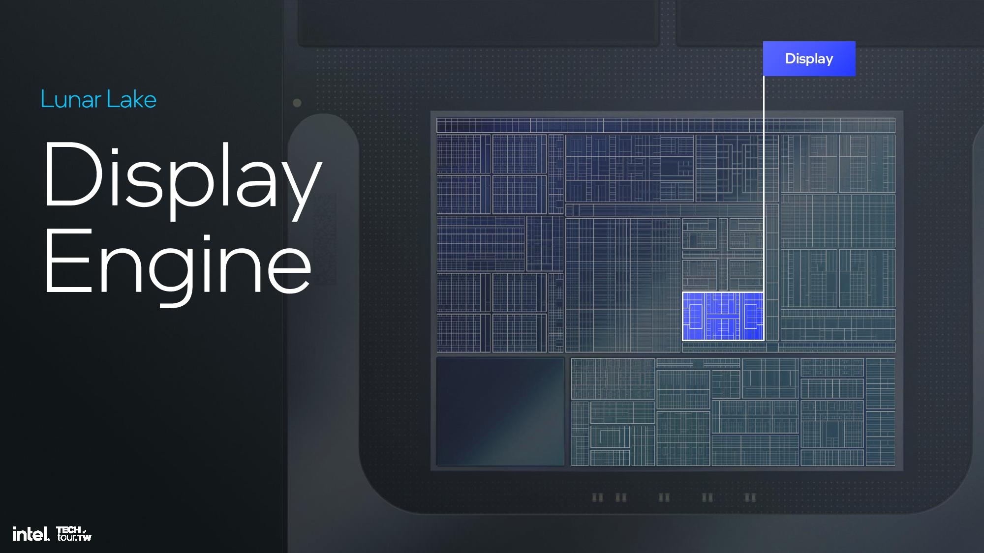
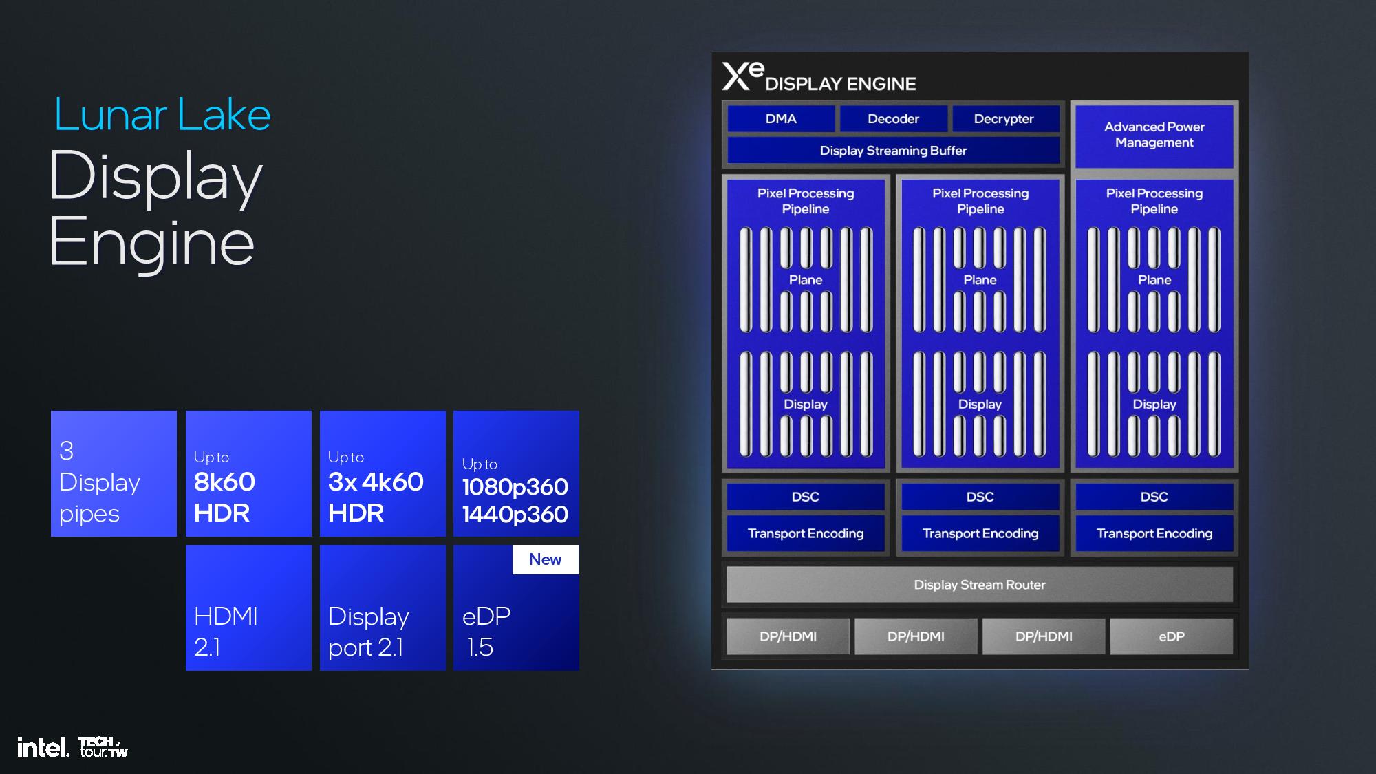
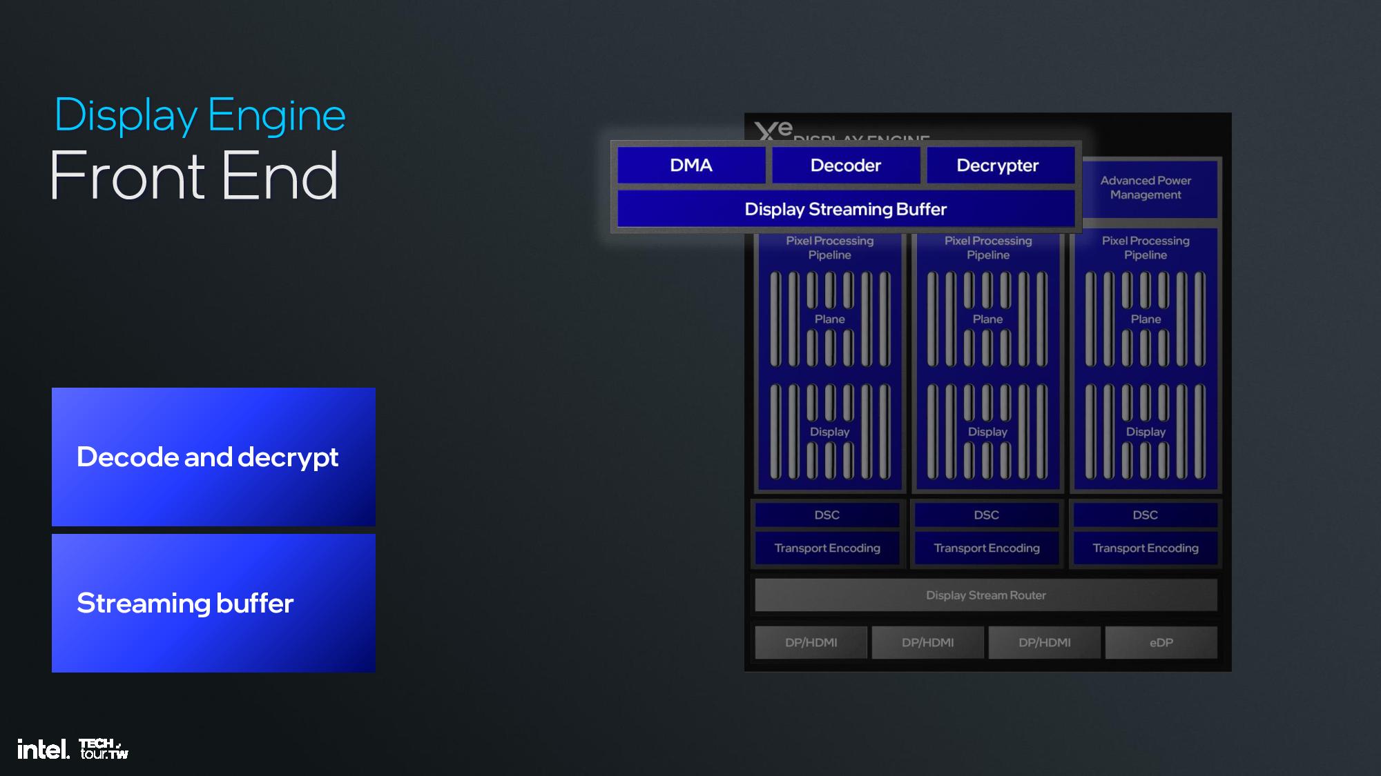
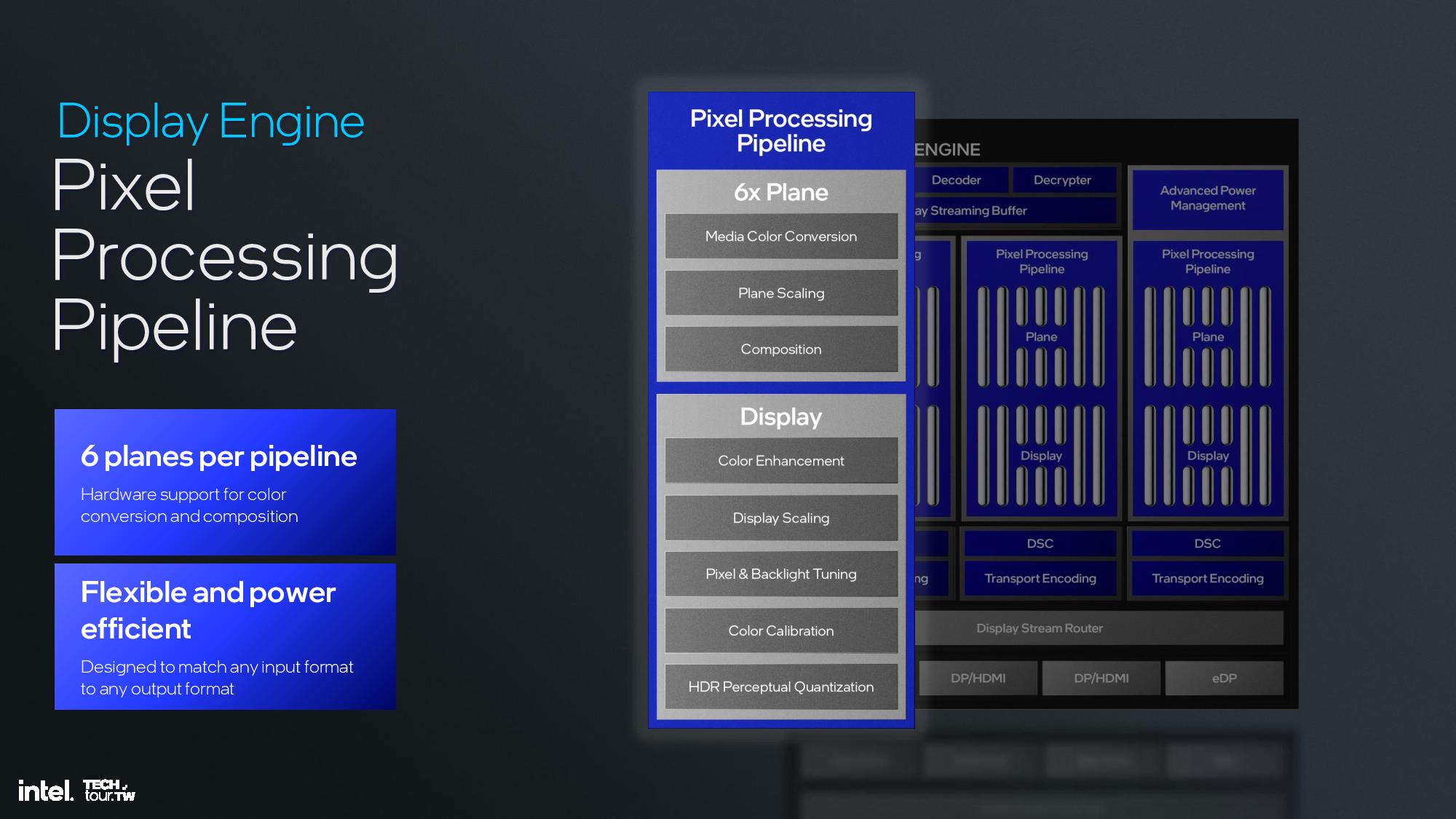
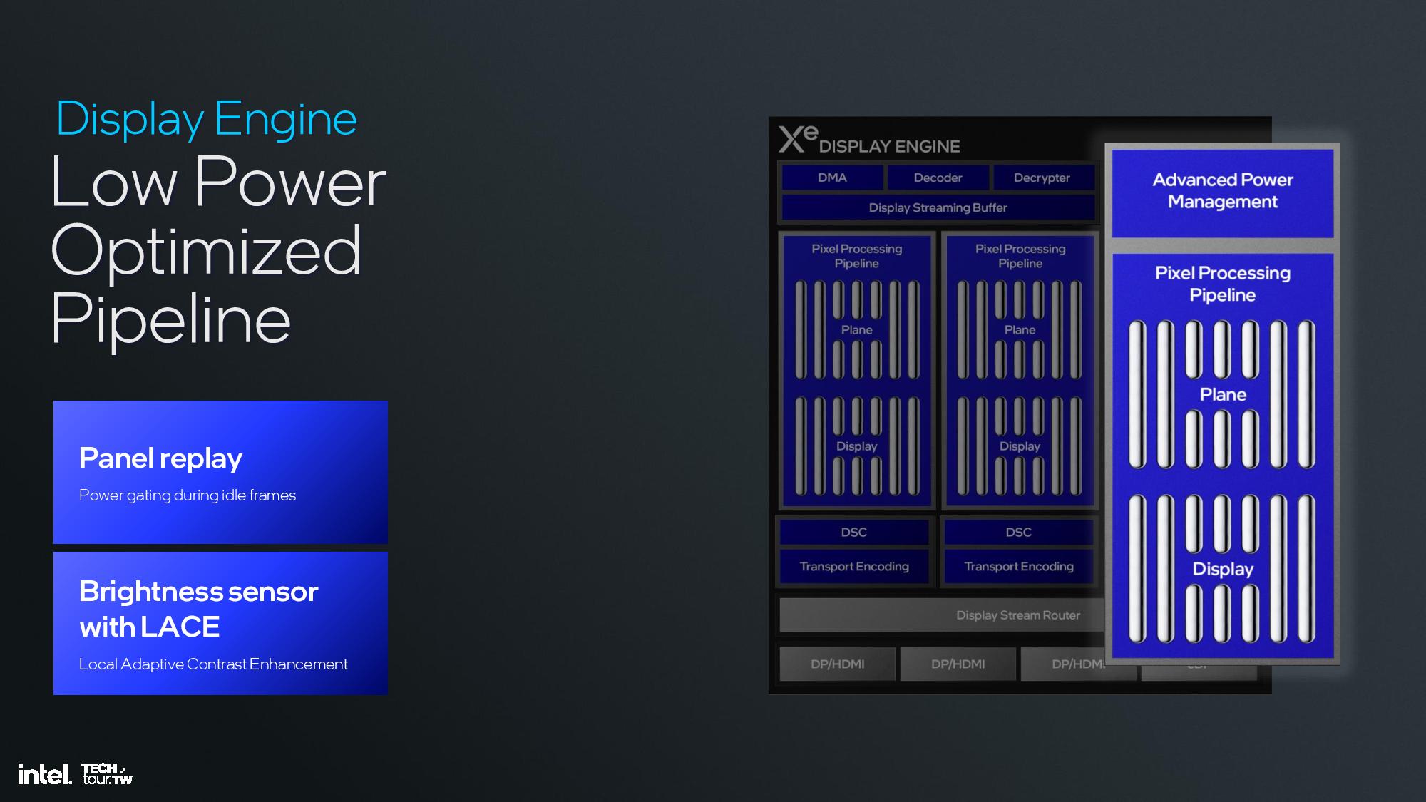
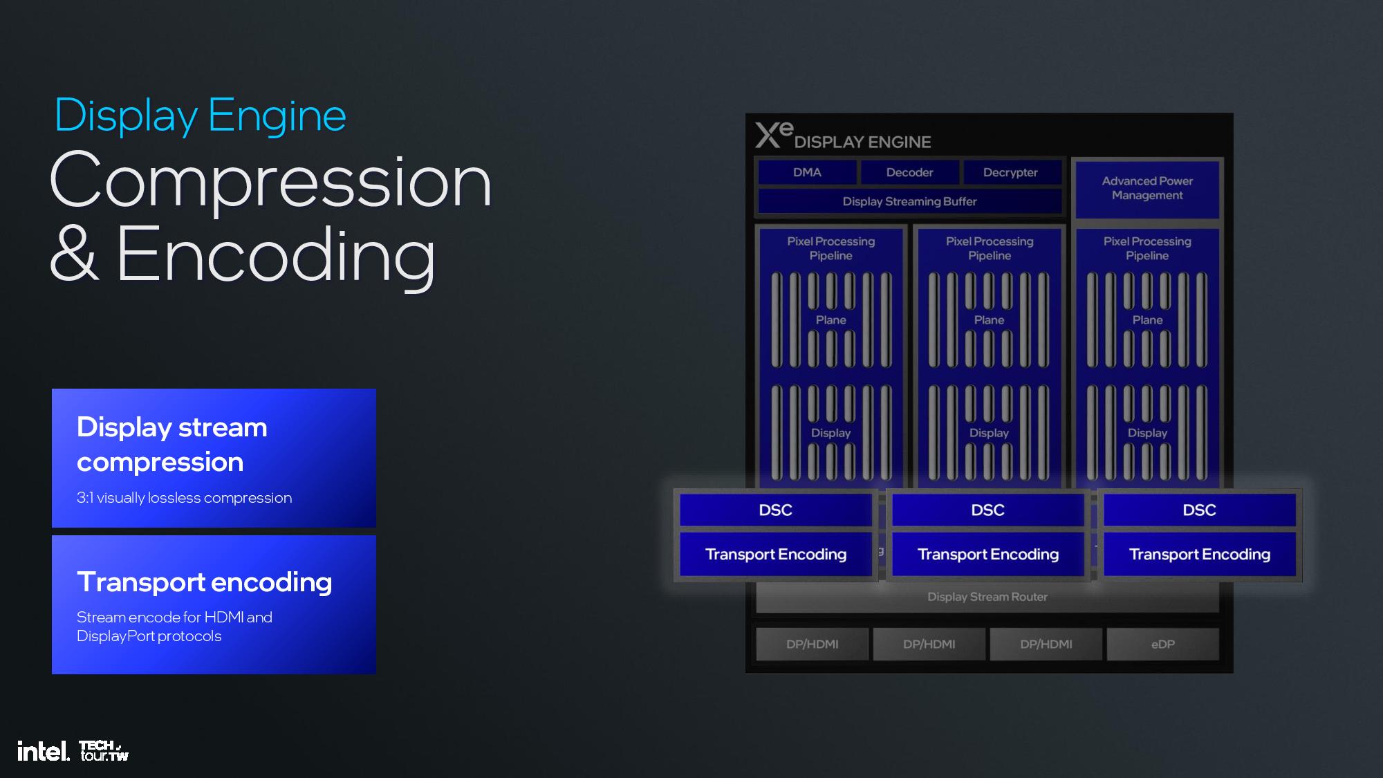
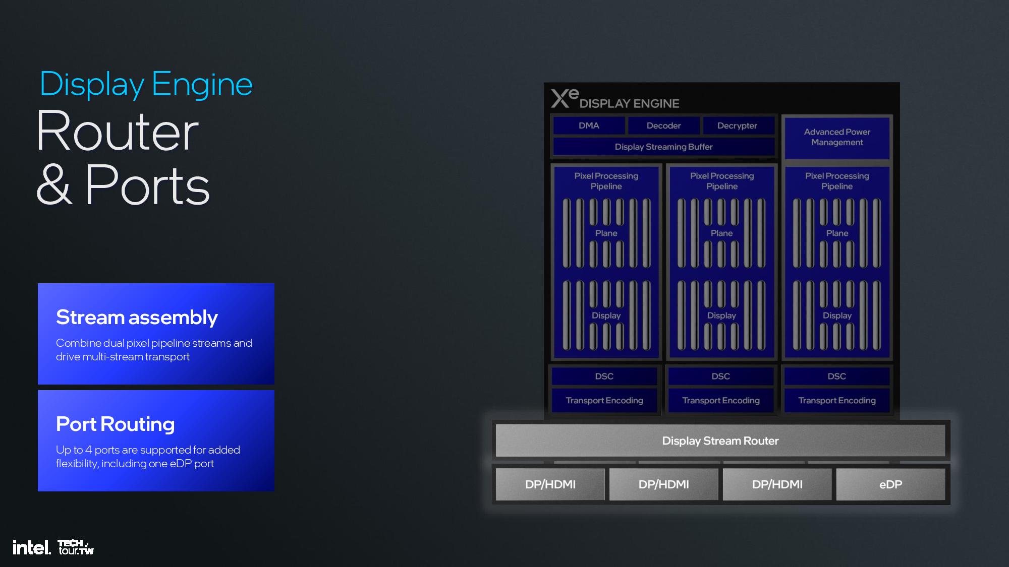
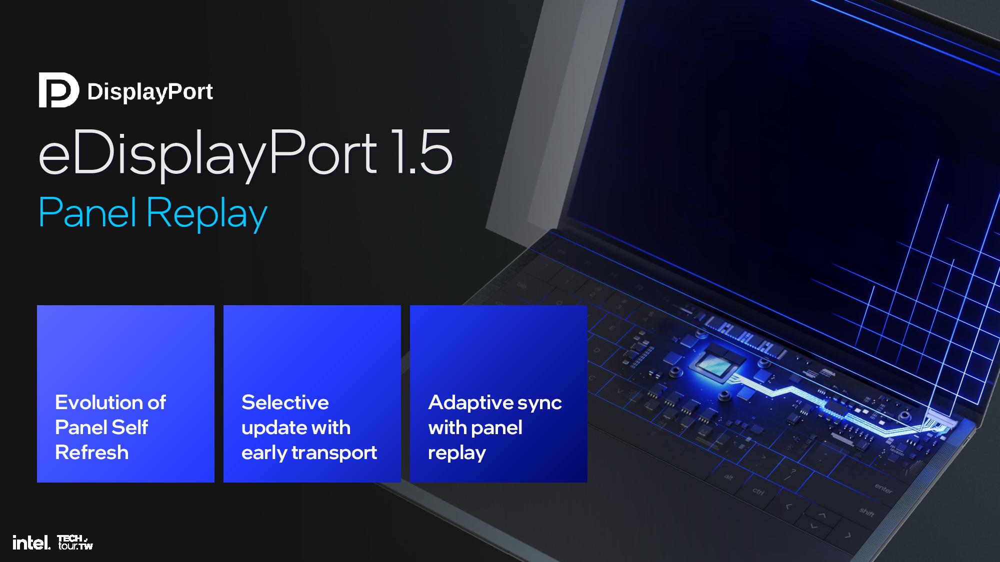
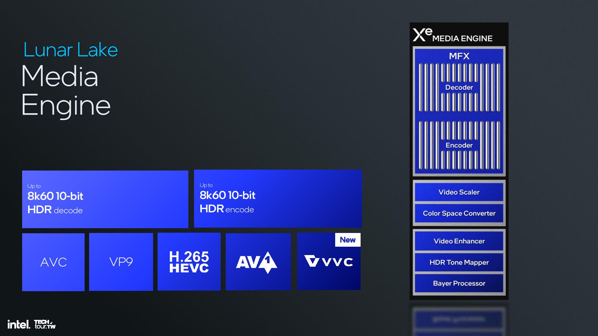
The display engine has three display pipes, up to 8K60 HDR, three 4K60 HDR displays, and up to 1080p360 and 1440p360. Outputs include HDMI 2.1, DisplayPort 2.1, and eDP 1.5. You can see the details of the graphics engine pipeline in the slides above.
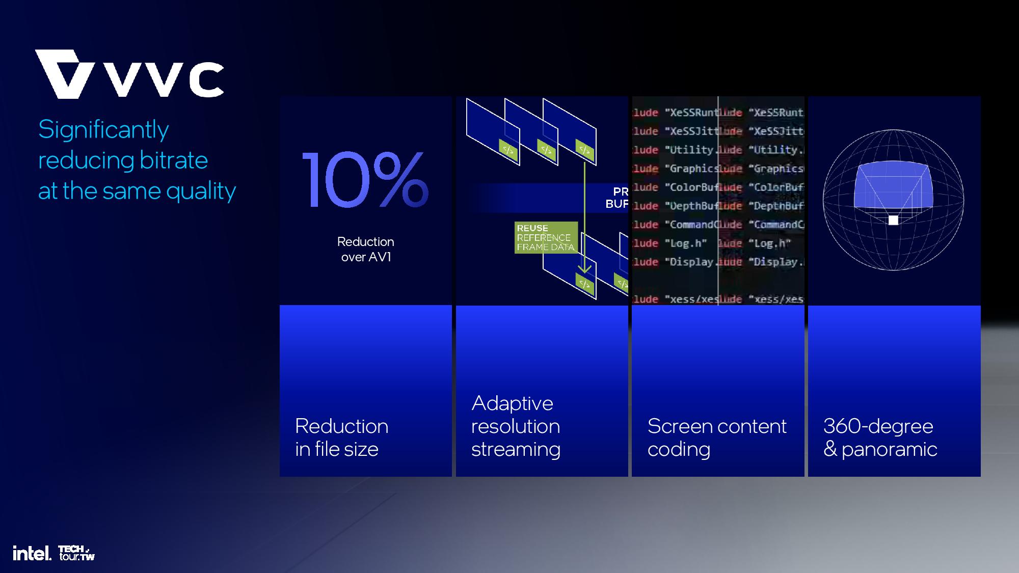
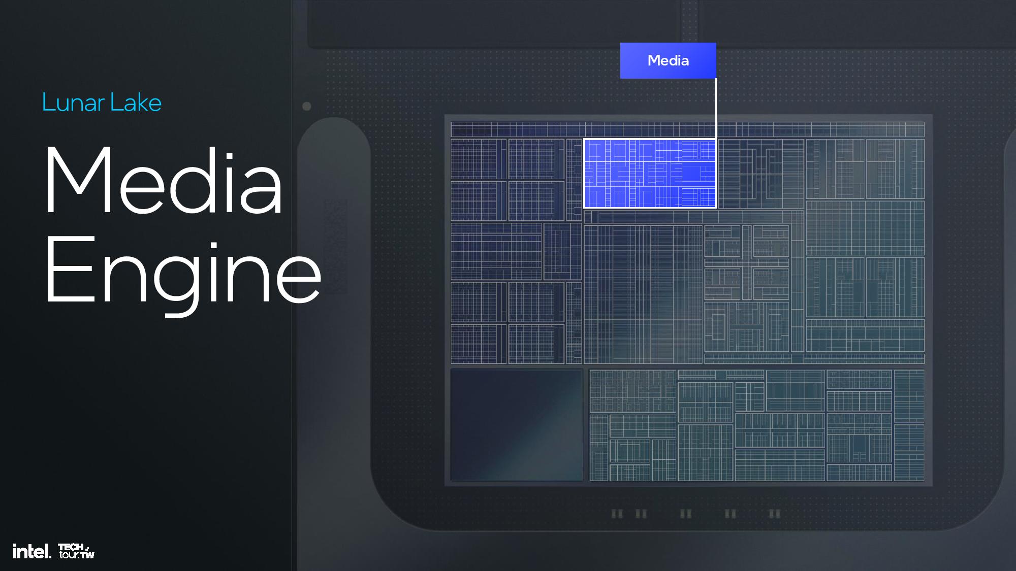
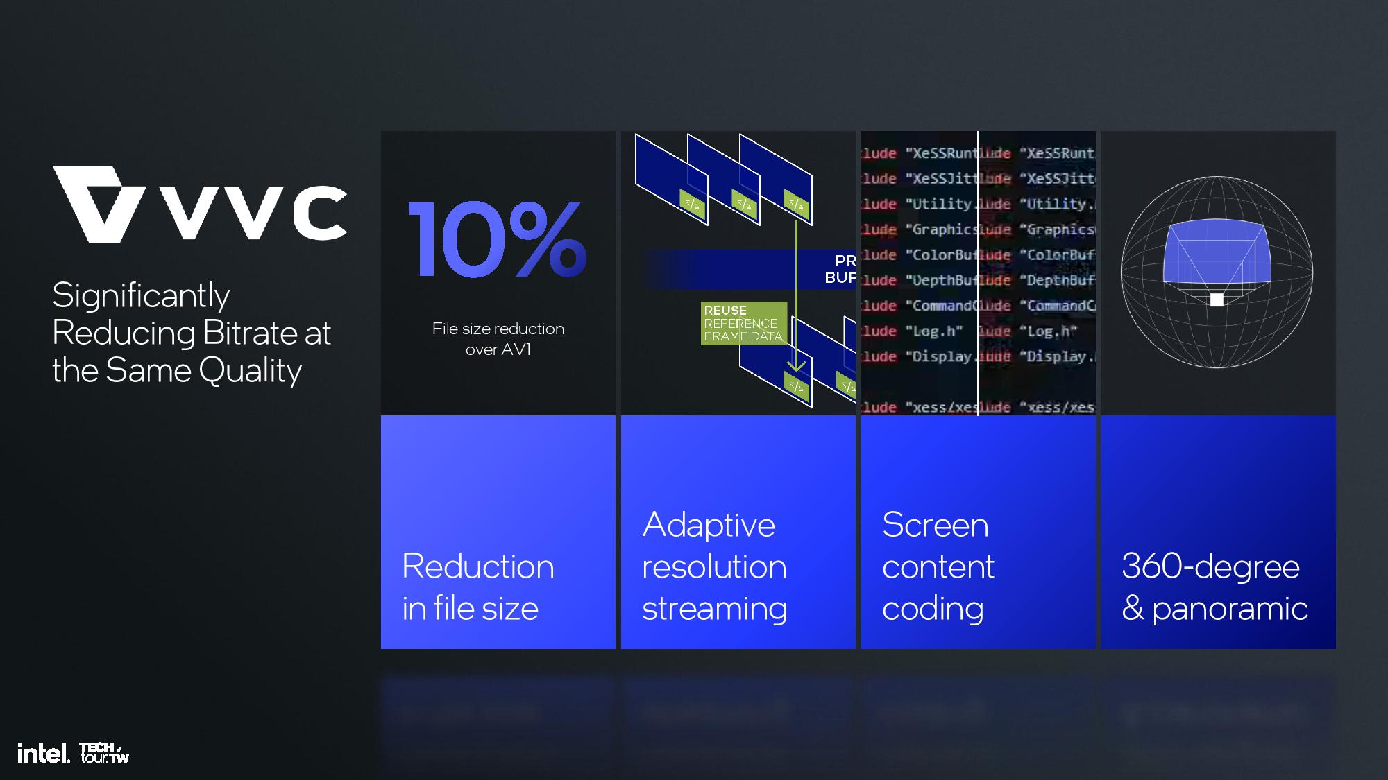
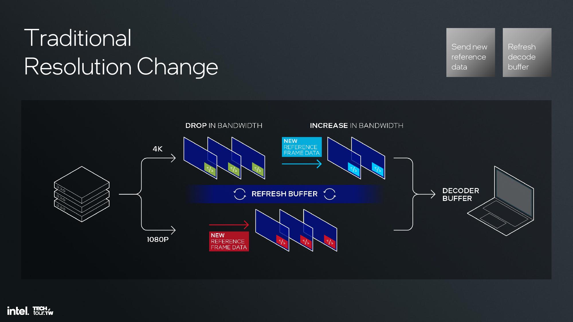
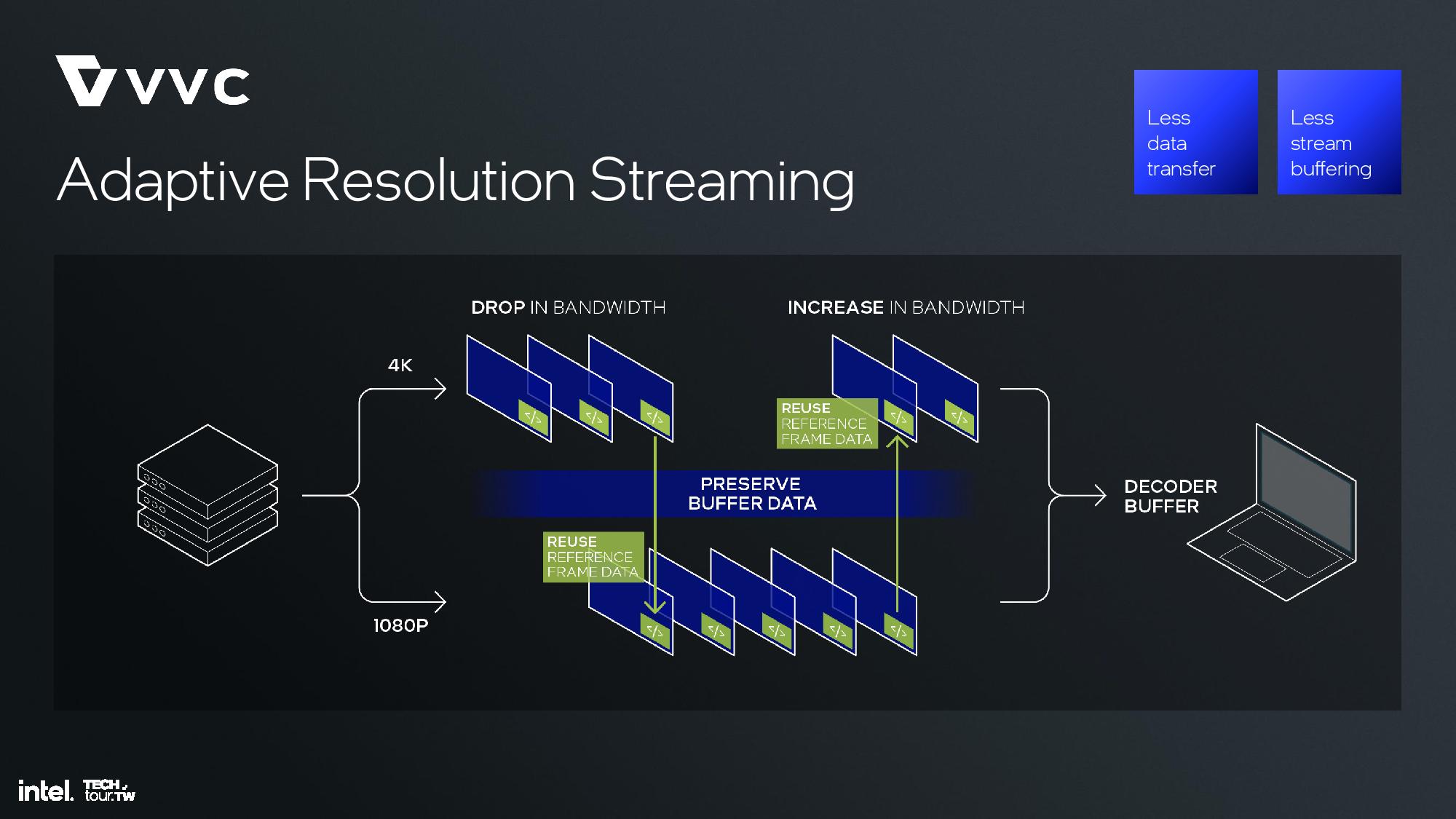
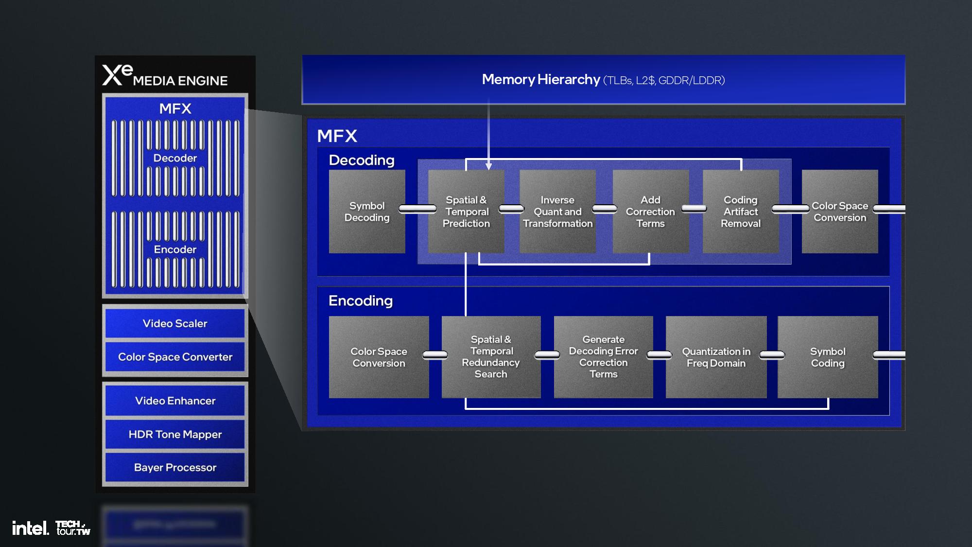
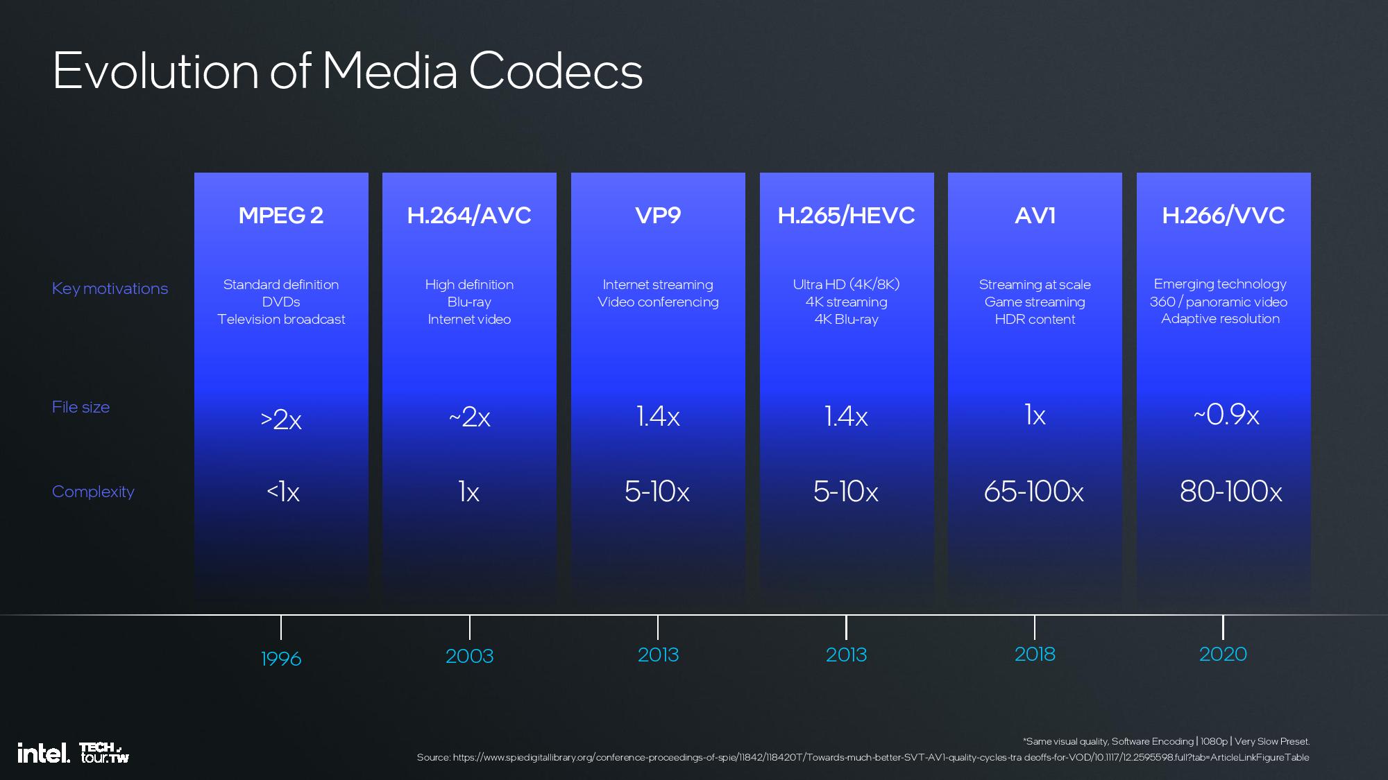
The memory side cache provides 8MB to store some of the media information to increase bandwidth and save power. The media engine supports up to 8K60 10-bit HDR decode and encode, along with support for all of the media standards, along with the new H.266/VVC codec — but only for decode.
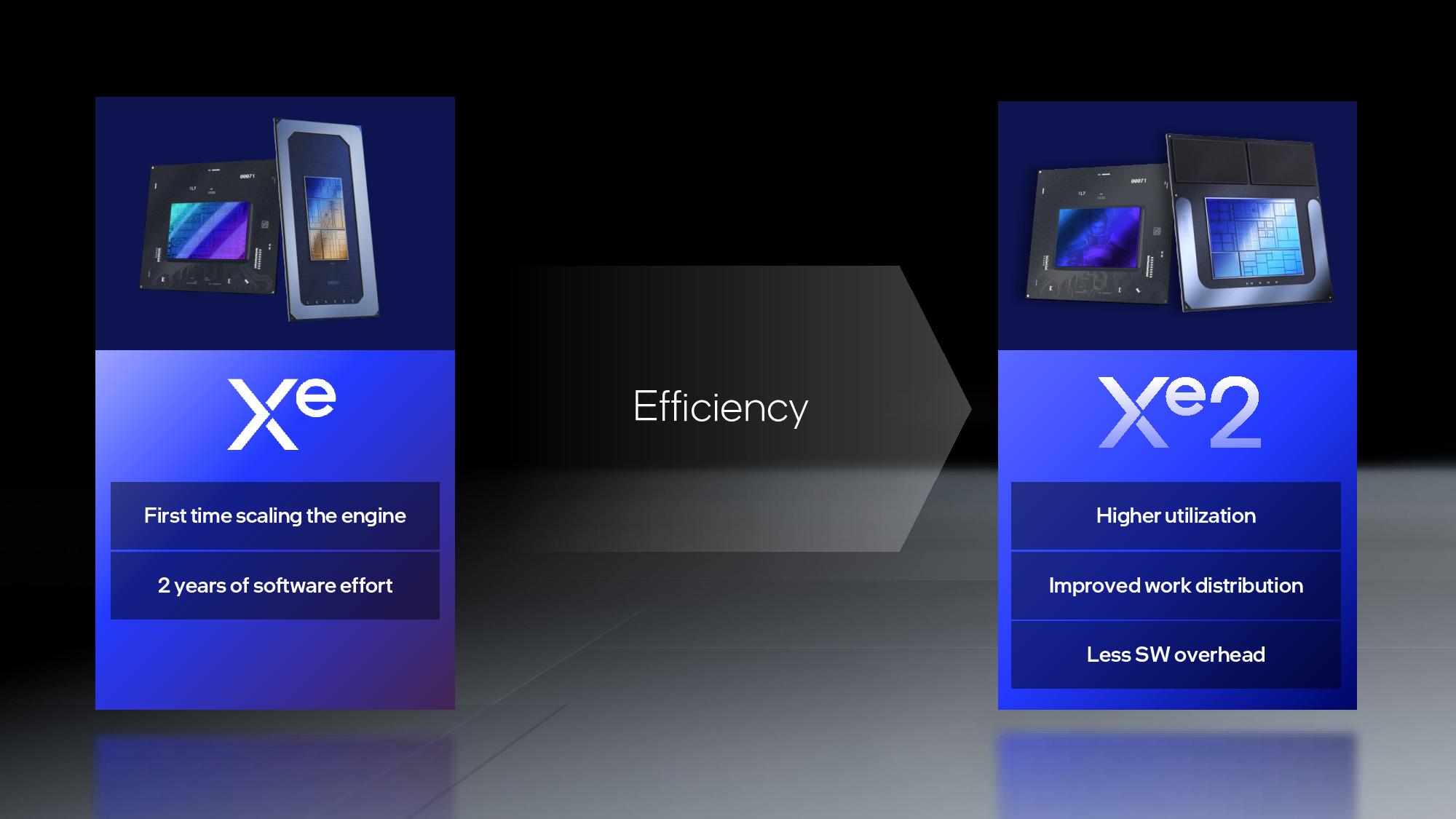
And of course, all of the new graphics features are backed by the past couple of years of effort by Intel's GPU drivers team. Arc GPUs first arrived in 2022 and had plenty of early growing pains. The latest drivers have come a long way, and Xe2 should benefit from everything that came before, with some improvements in the core architecture to remove bottleneck and limitations present in the first generation of Xe Graphics.
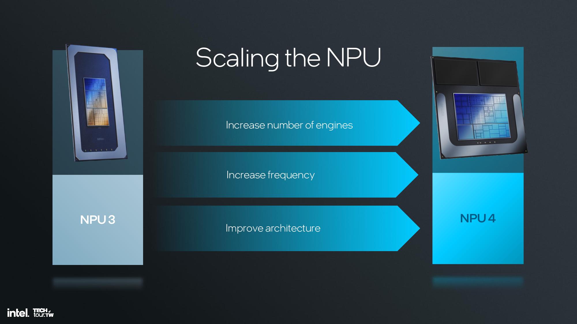
Lunar Lake NPU 4.0
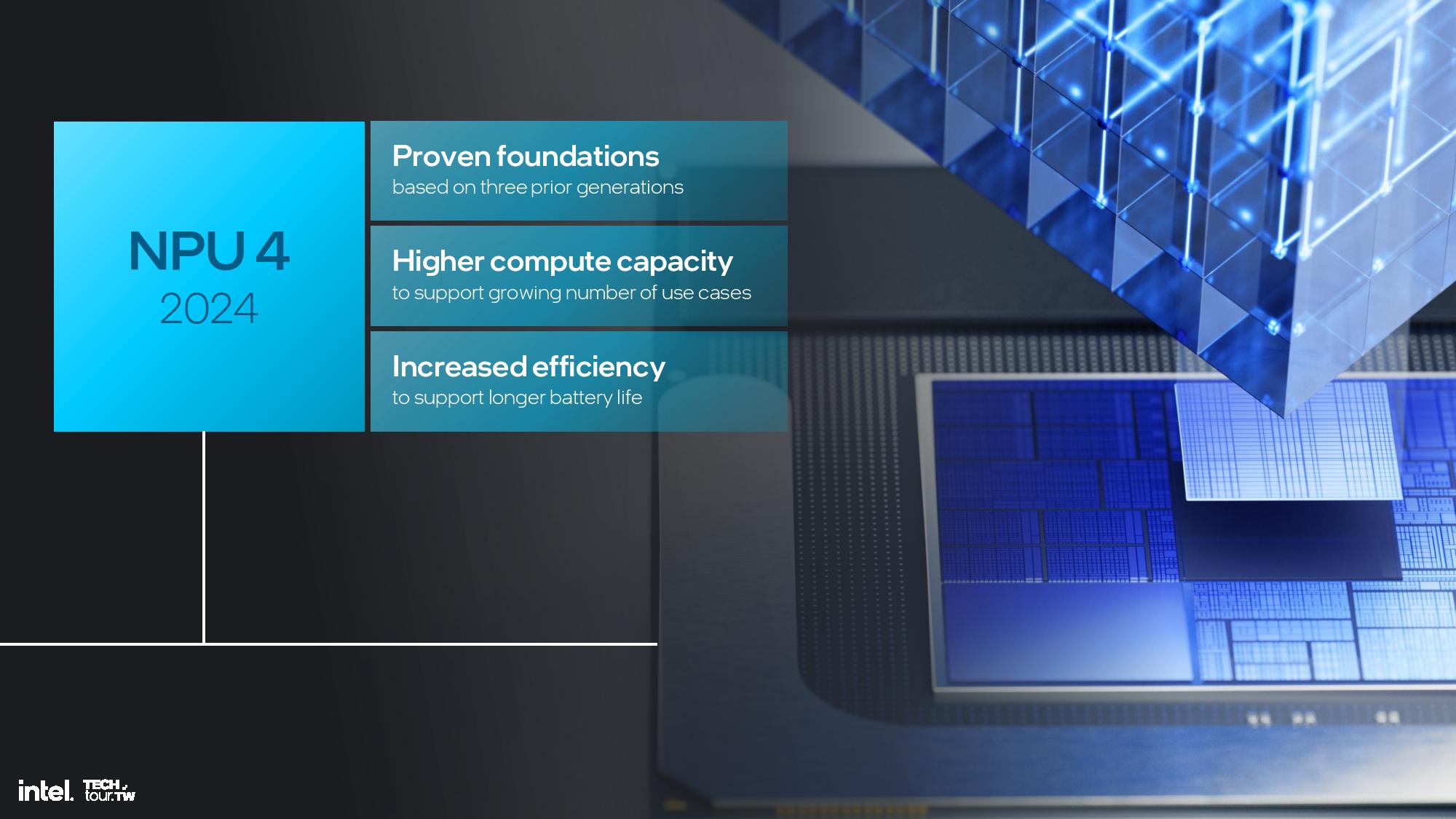
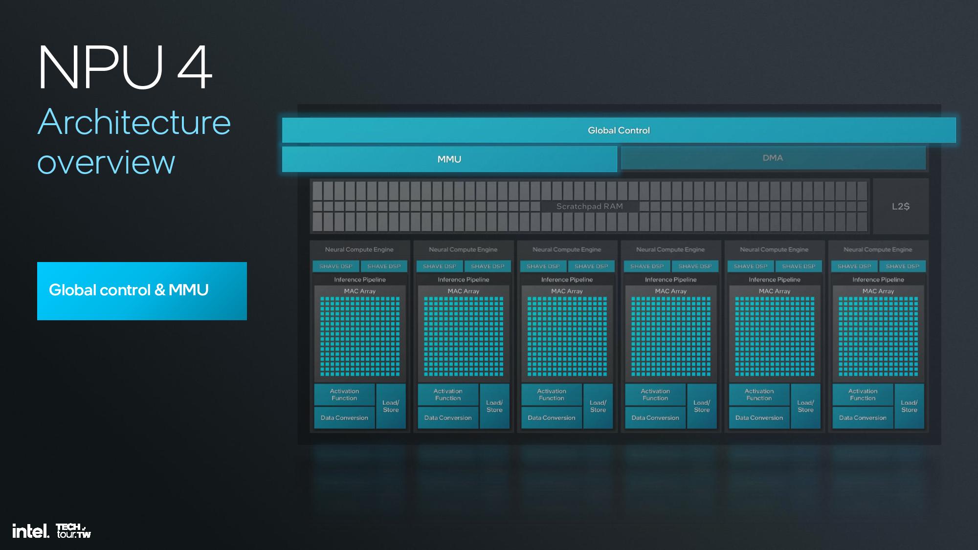
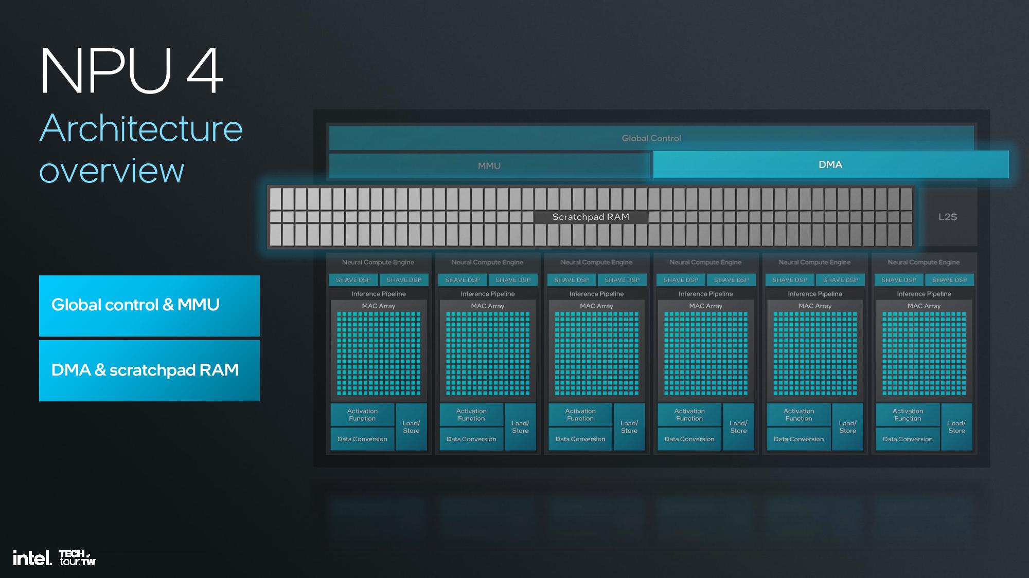
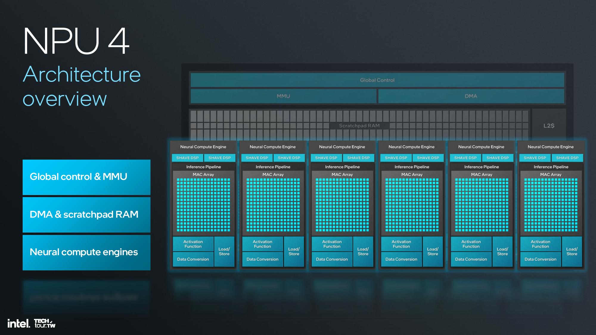
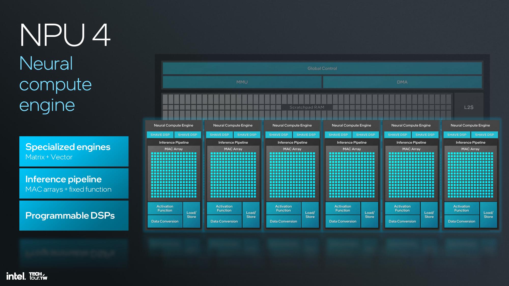
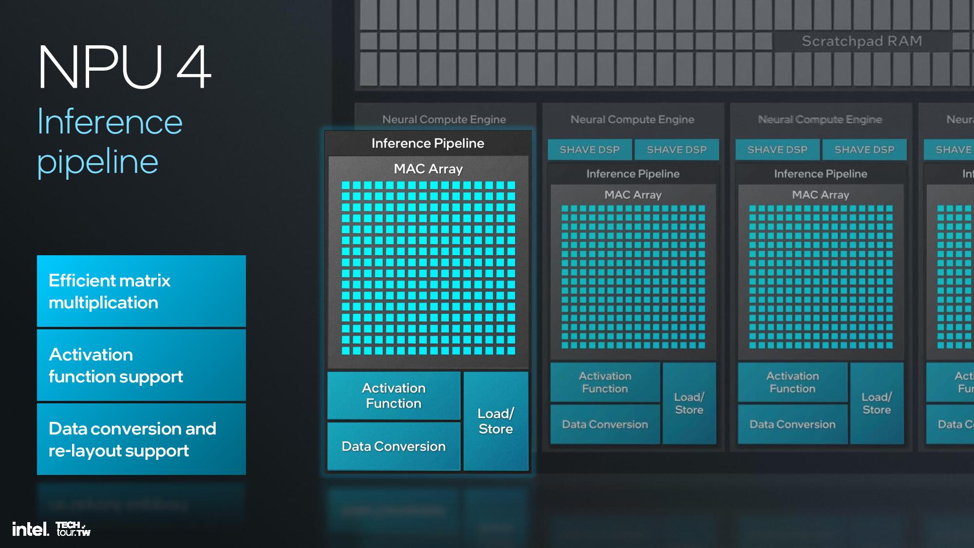
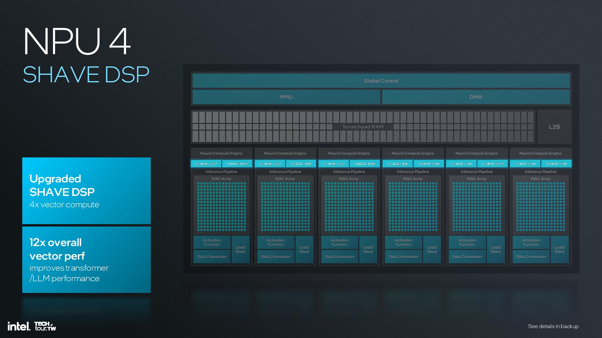
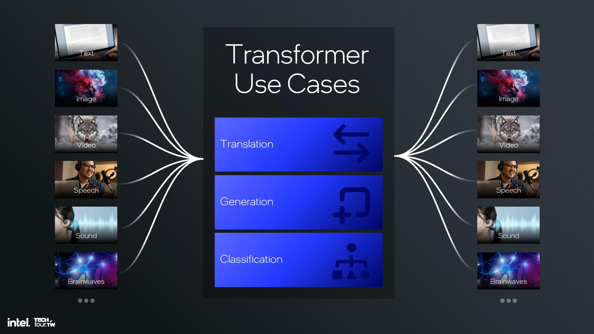
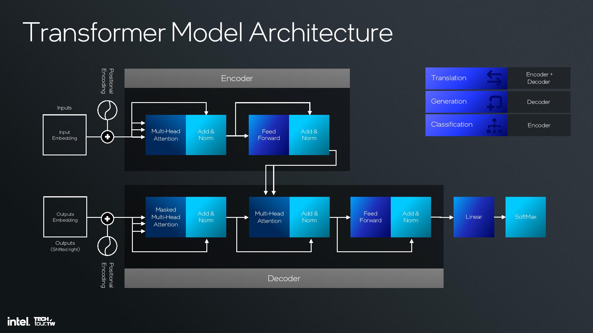
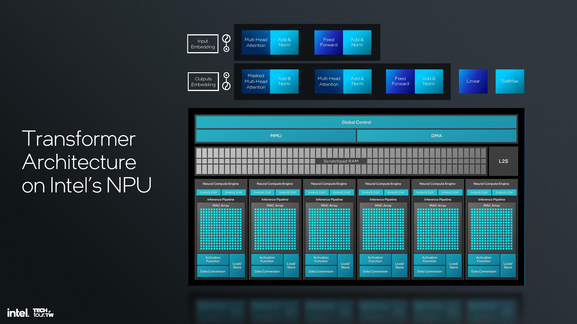
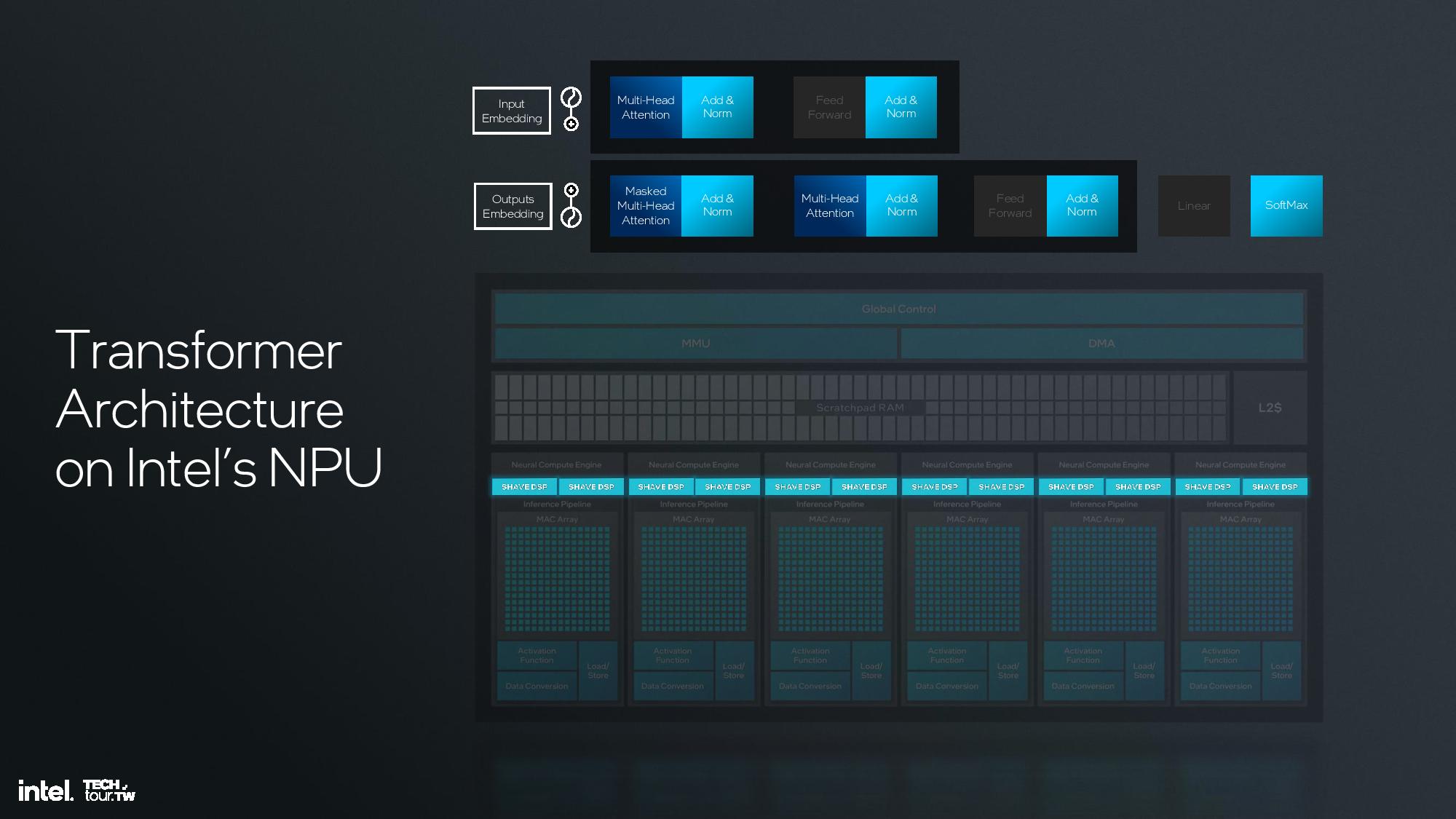
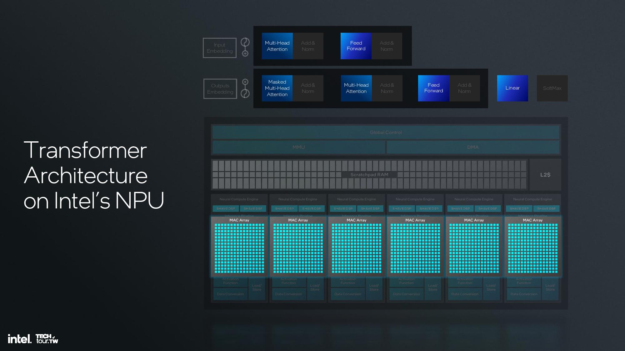
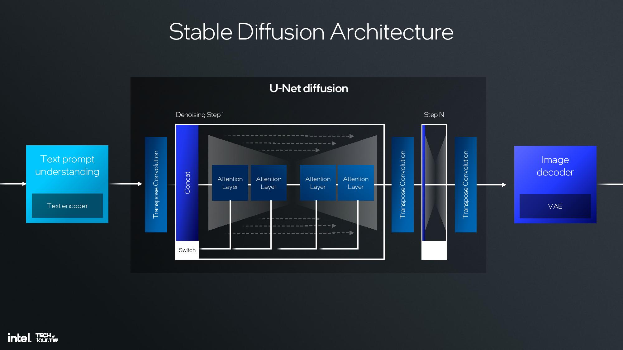
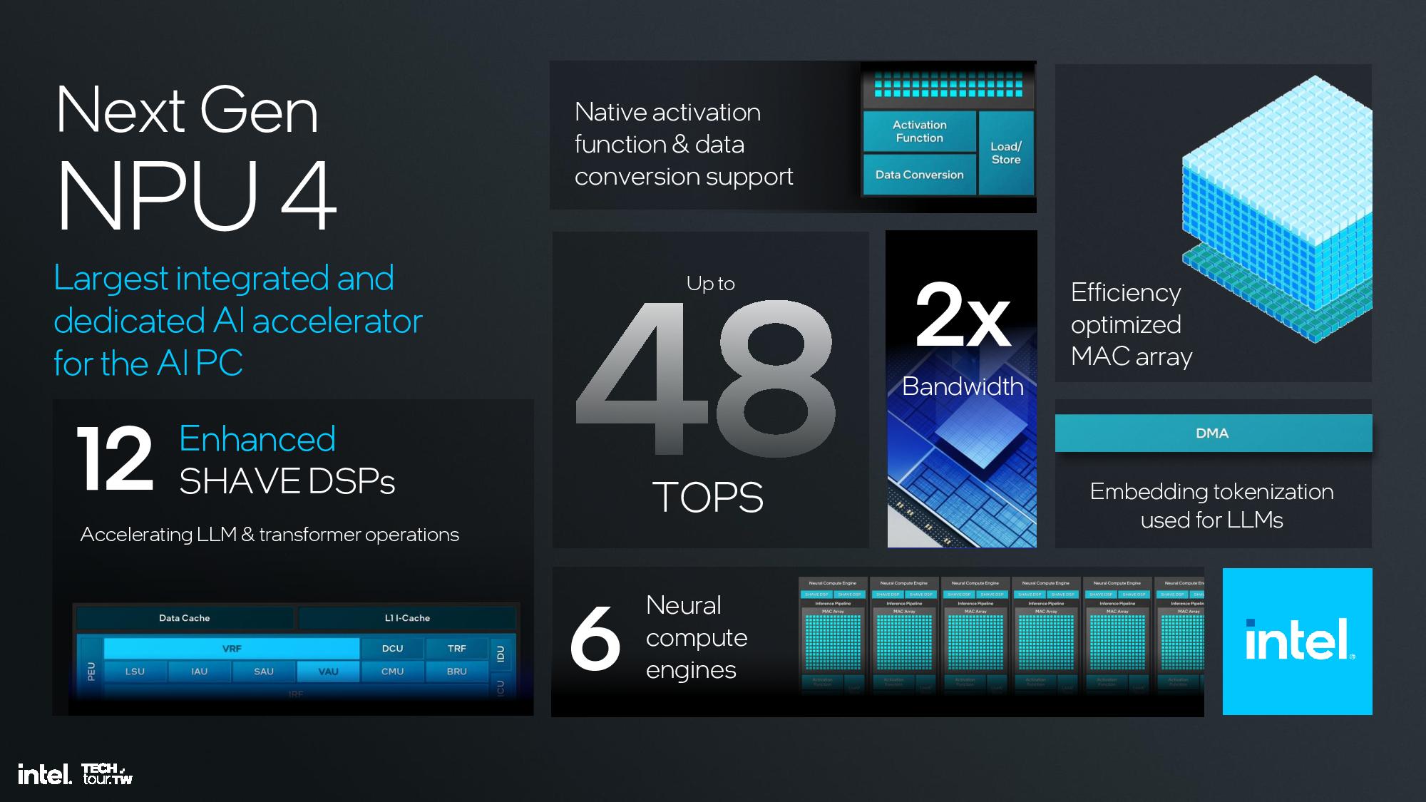


Intel shared deep dive architectural details of its fourth-gen NPU unit at the event, but I was unfortunately unable to attend this specific briefing. I do have a recording that I will watch and use to update this section, but for now I’ll have to let the slides do most of the talking.
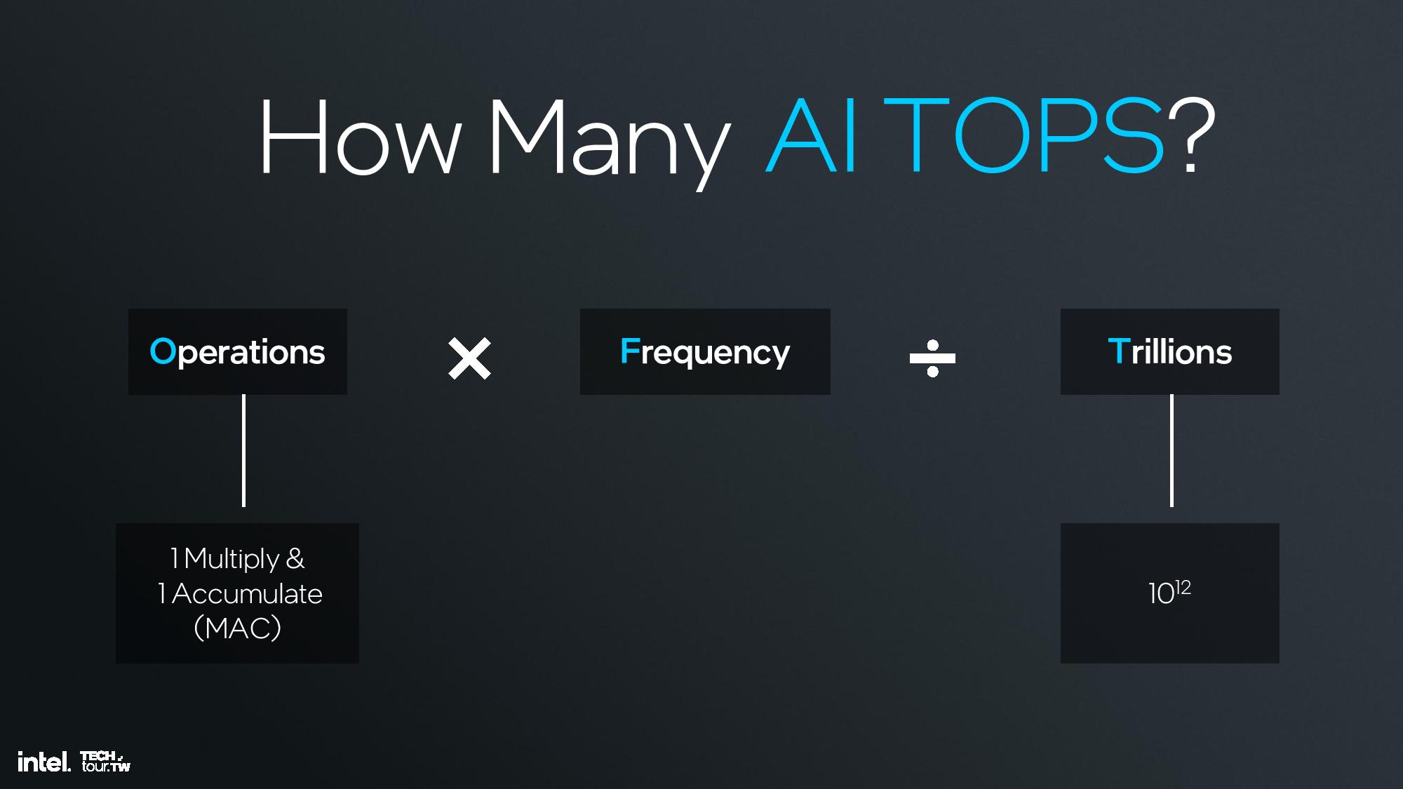
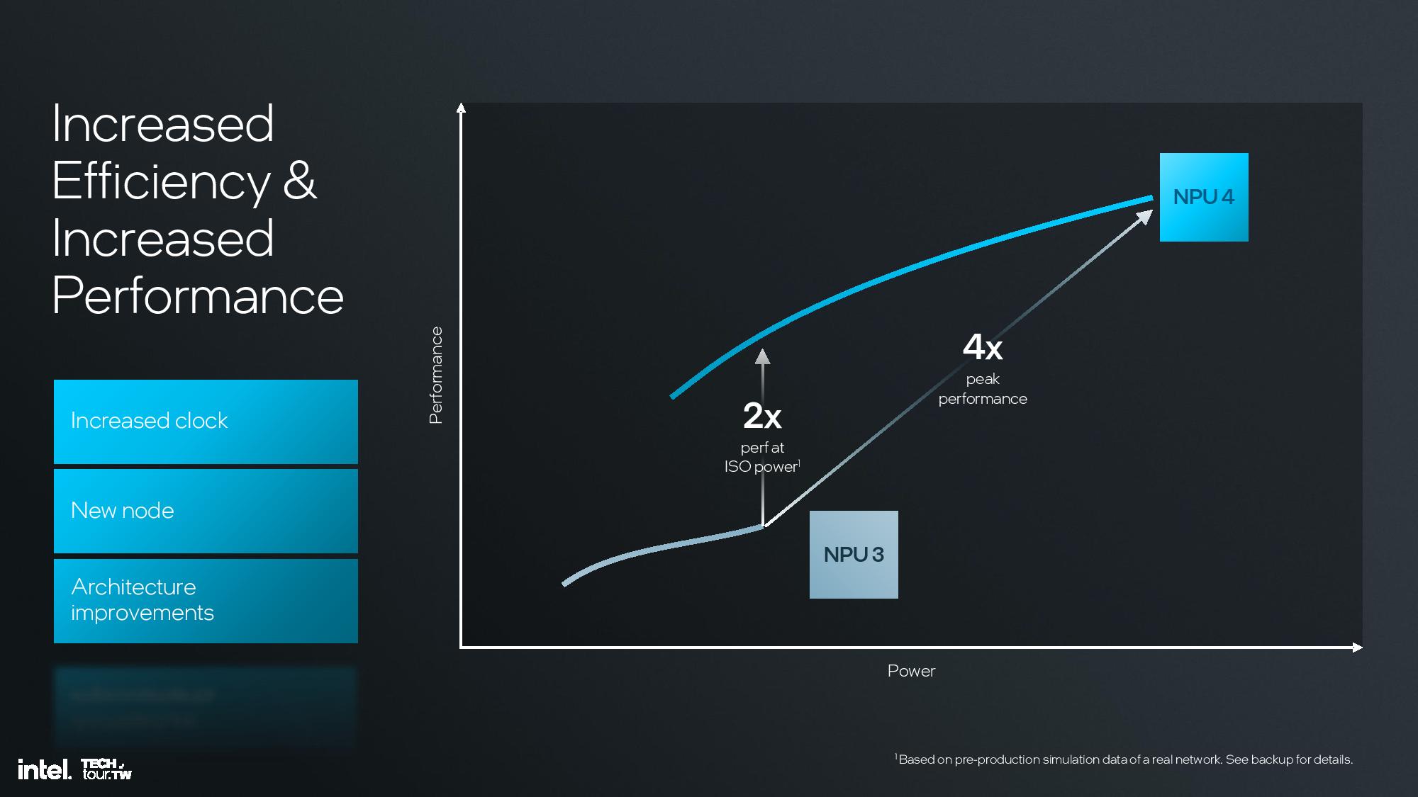
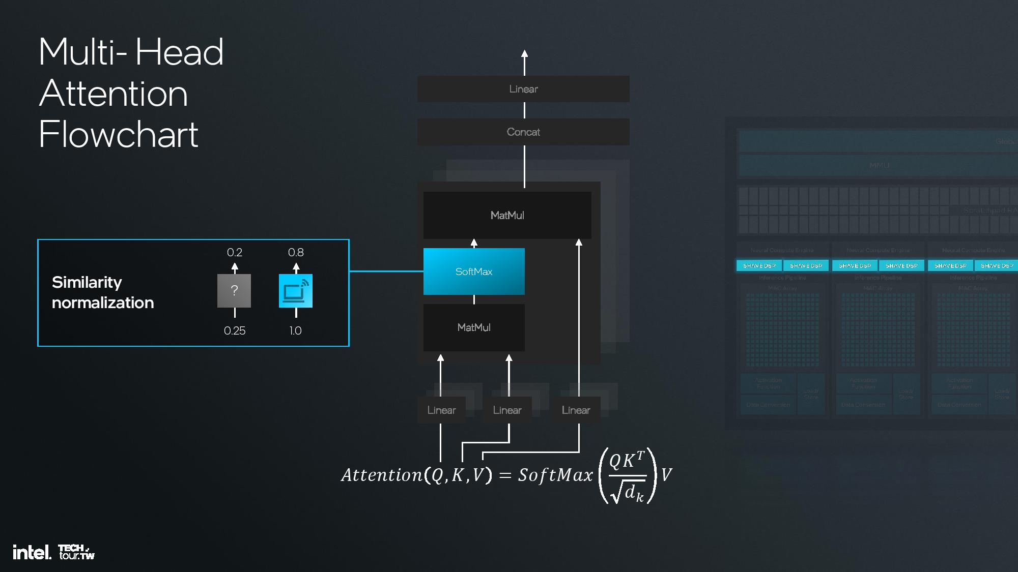
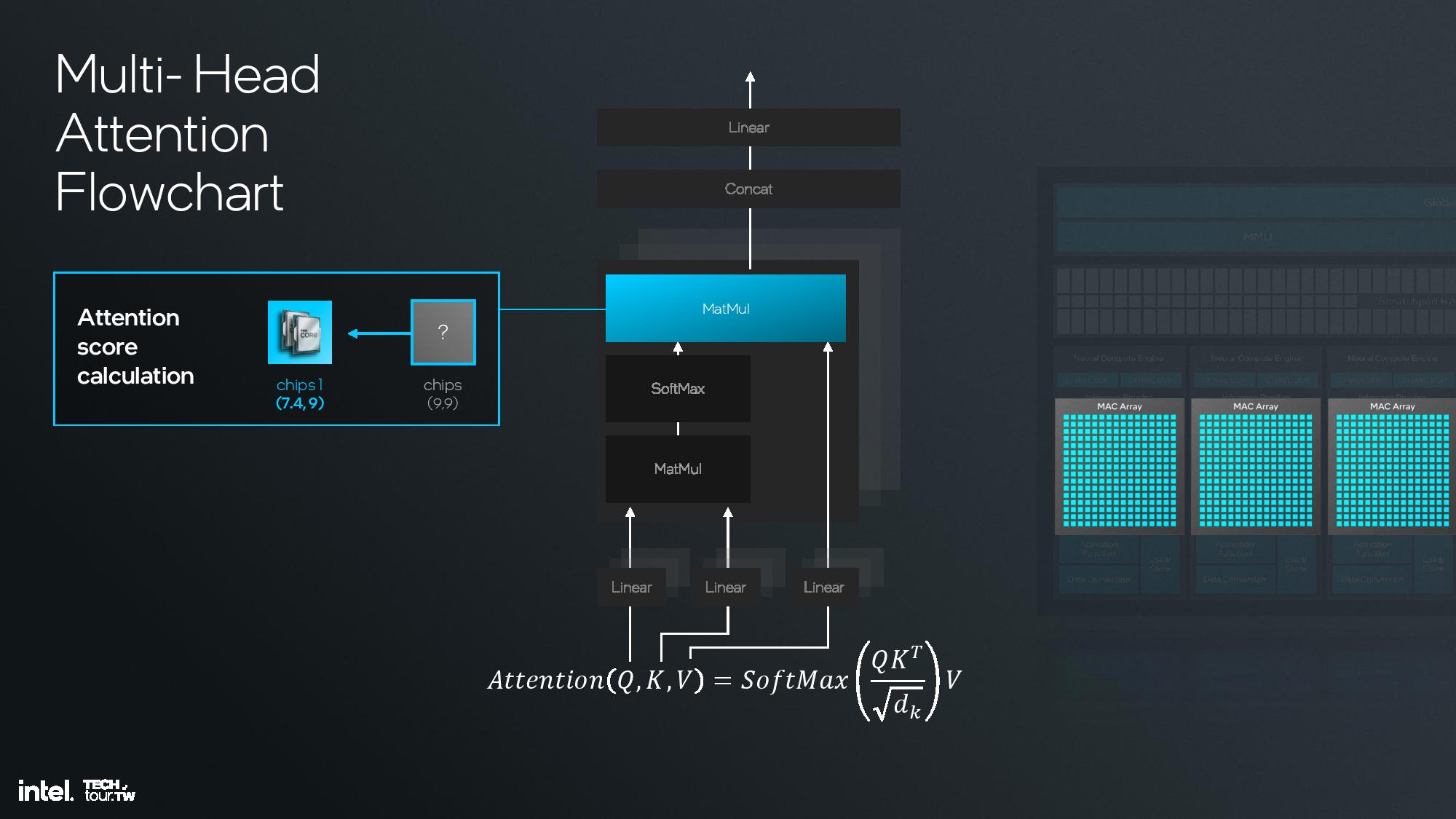
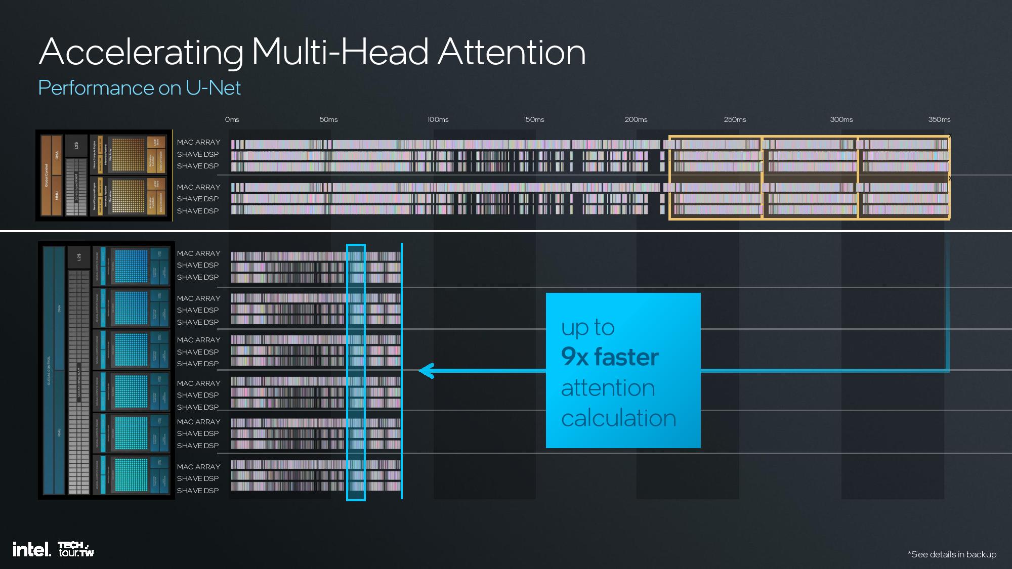
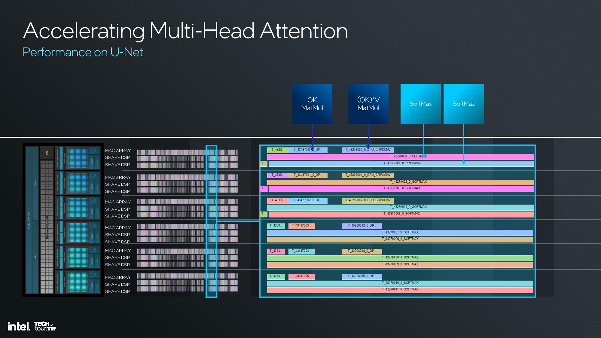
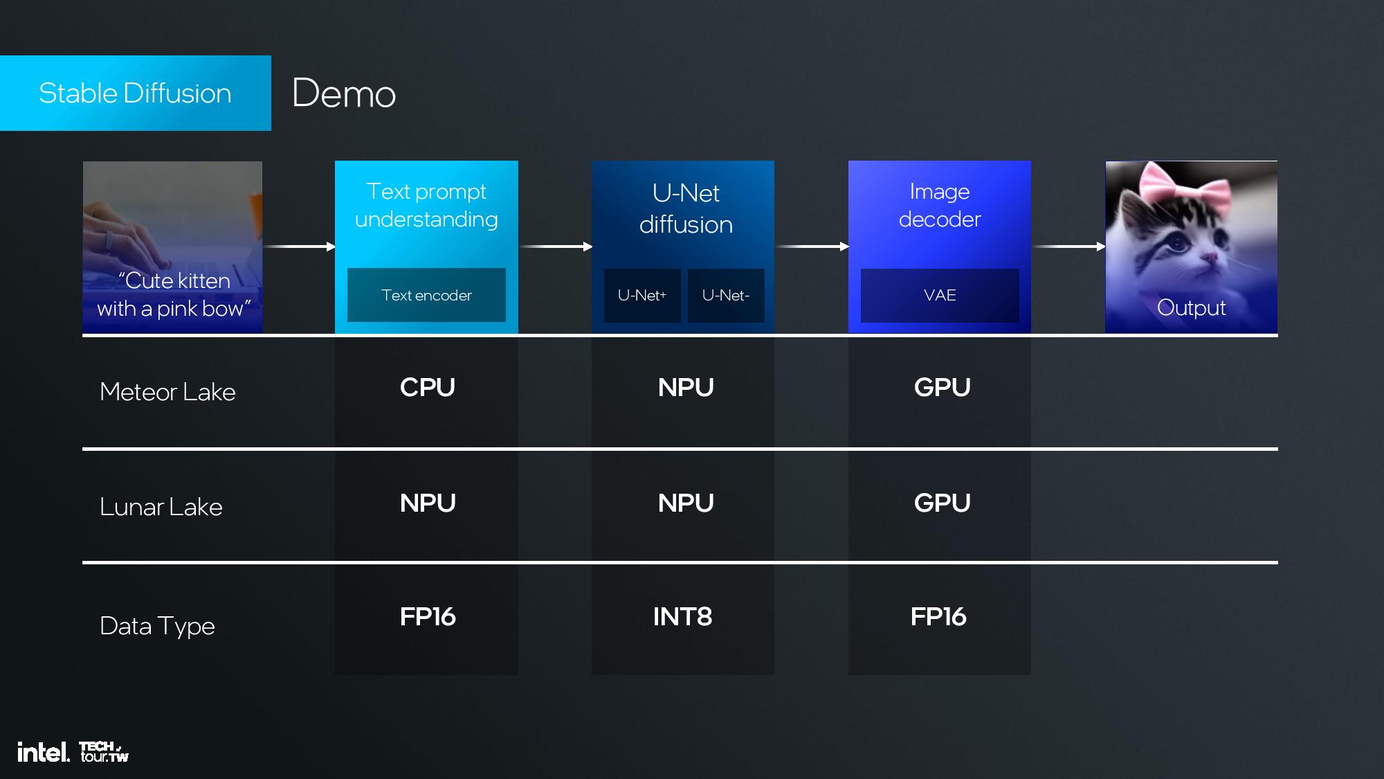
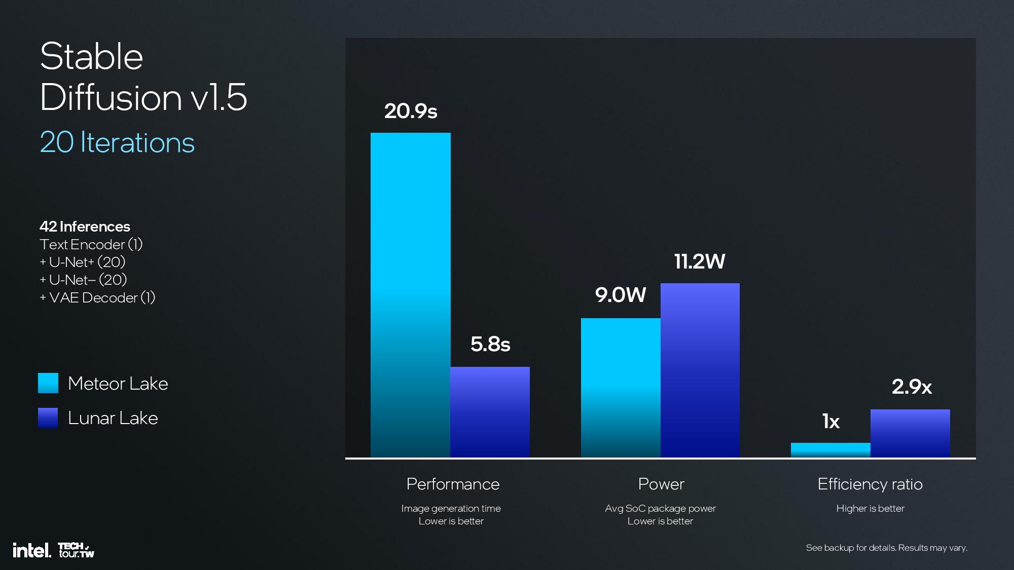
The NPU is the central component in Intel’s AI strategy, and with 48 TOPS of performance it easily meets Microsoft’s requirements for next-gen PCs. However, the NPU is primarily designed for AI offloading for low-intensity work, thus saving tremendous amounts of battery power. The GPU steps in for more demanding workloads with 67 TOPS of performance, while the CPU contributes another 5 TOPS. Overall, that gives Lunar Lake 120 total TOPS of AI performance.
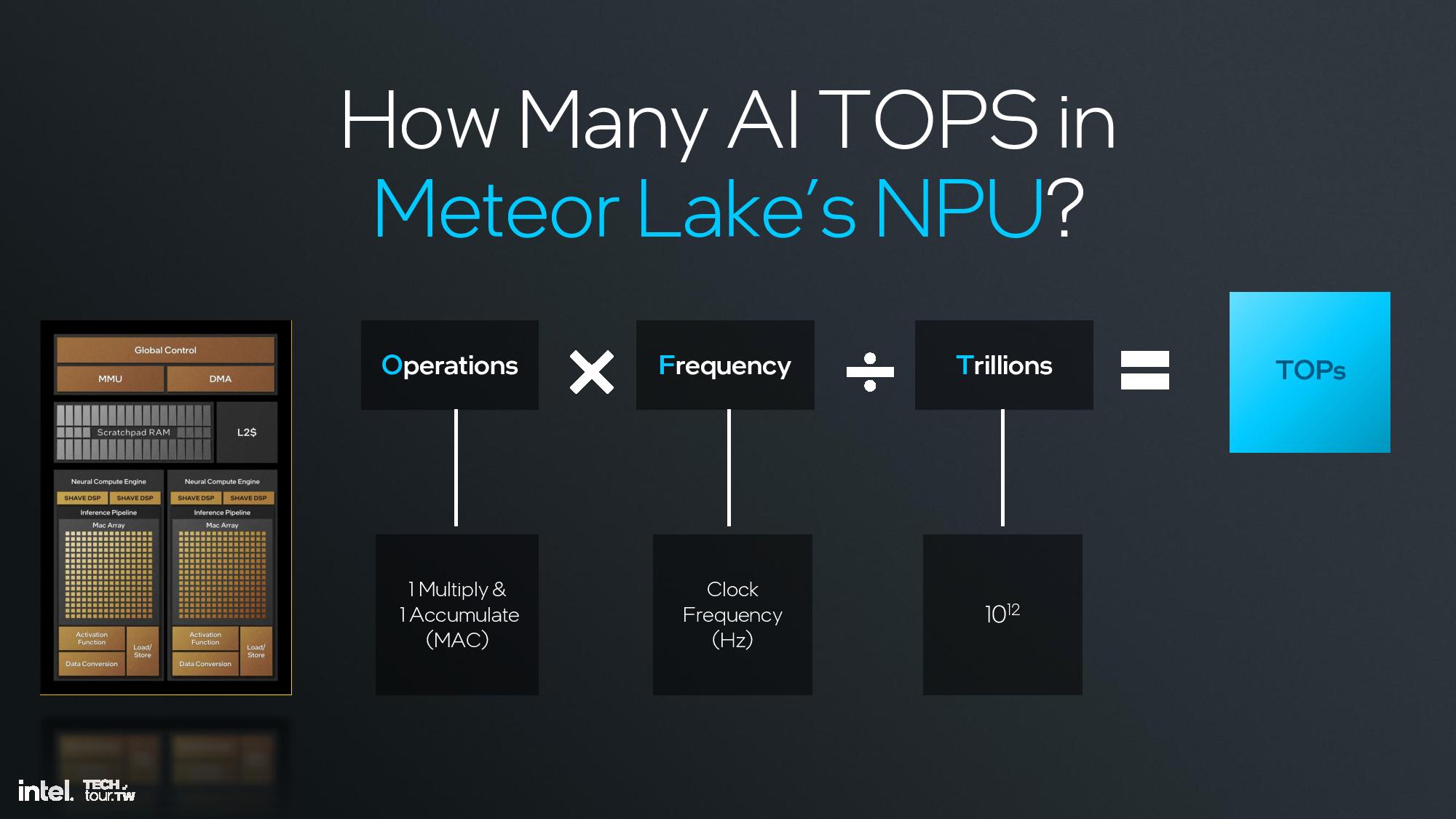
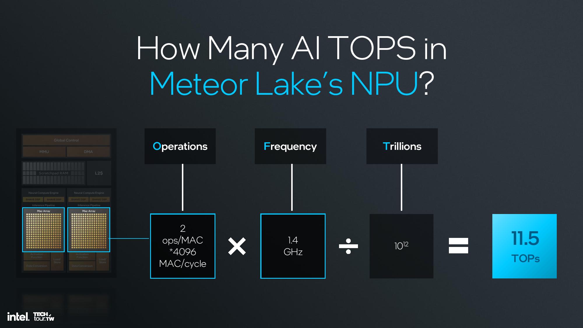
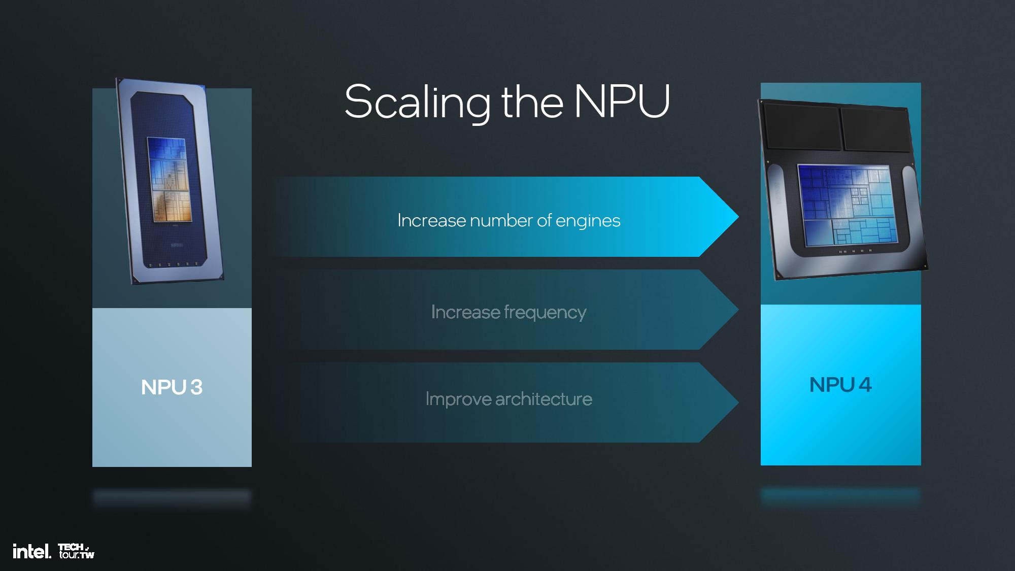
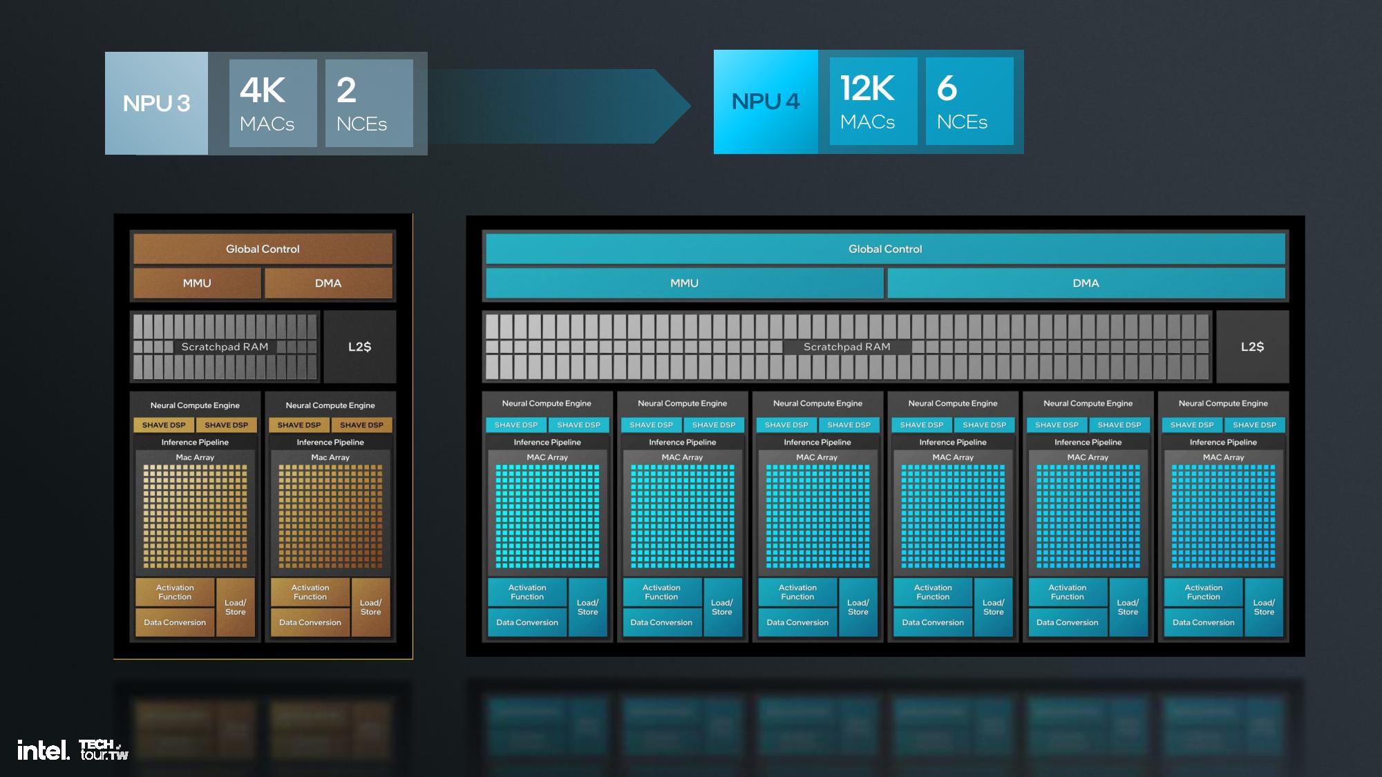
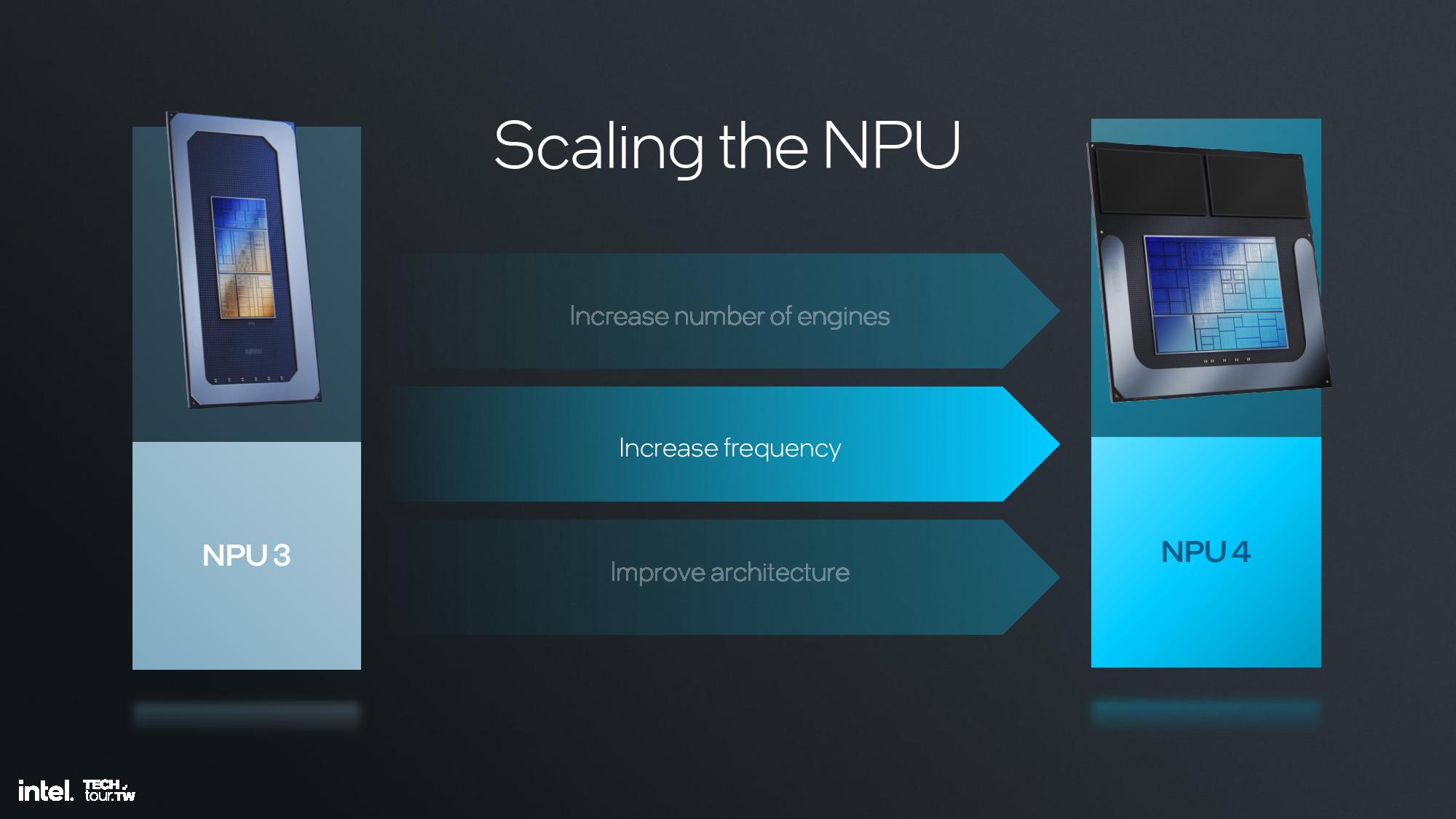
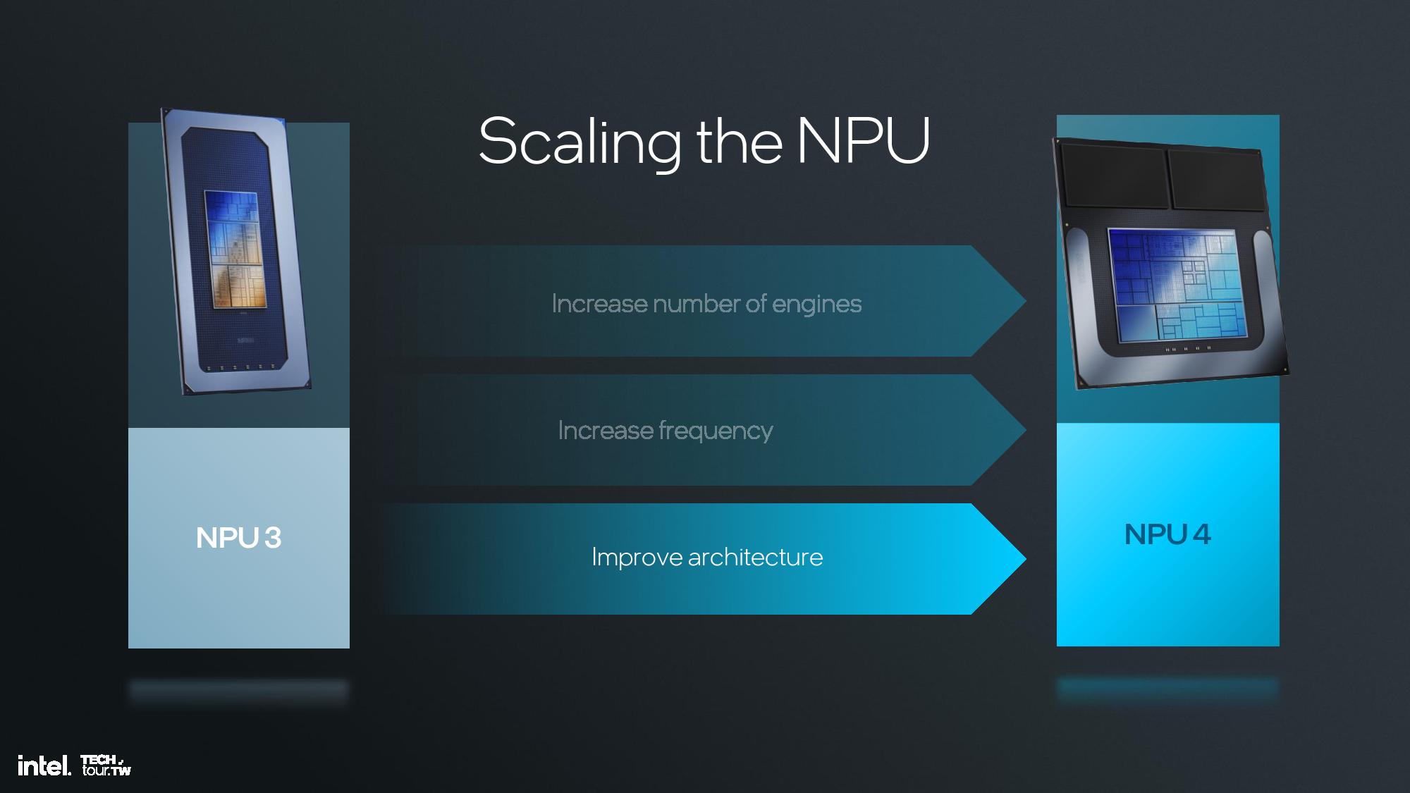
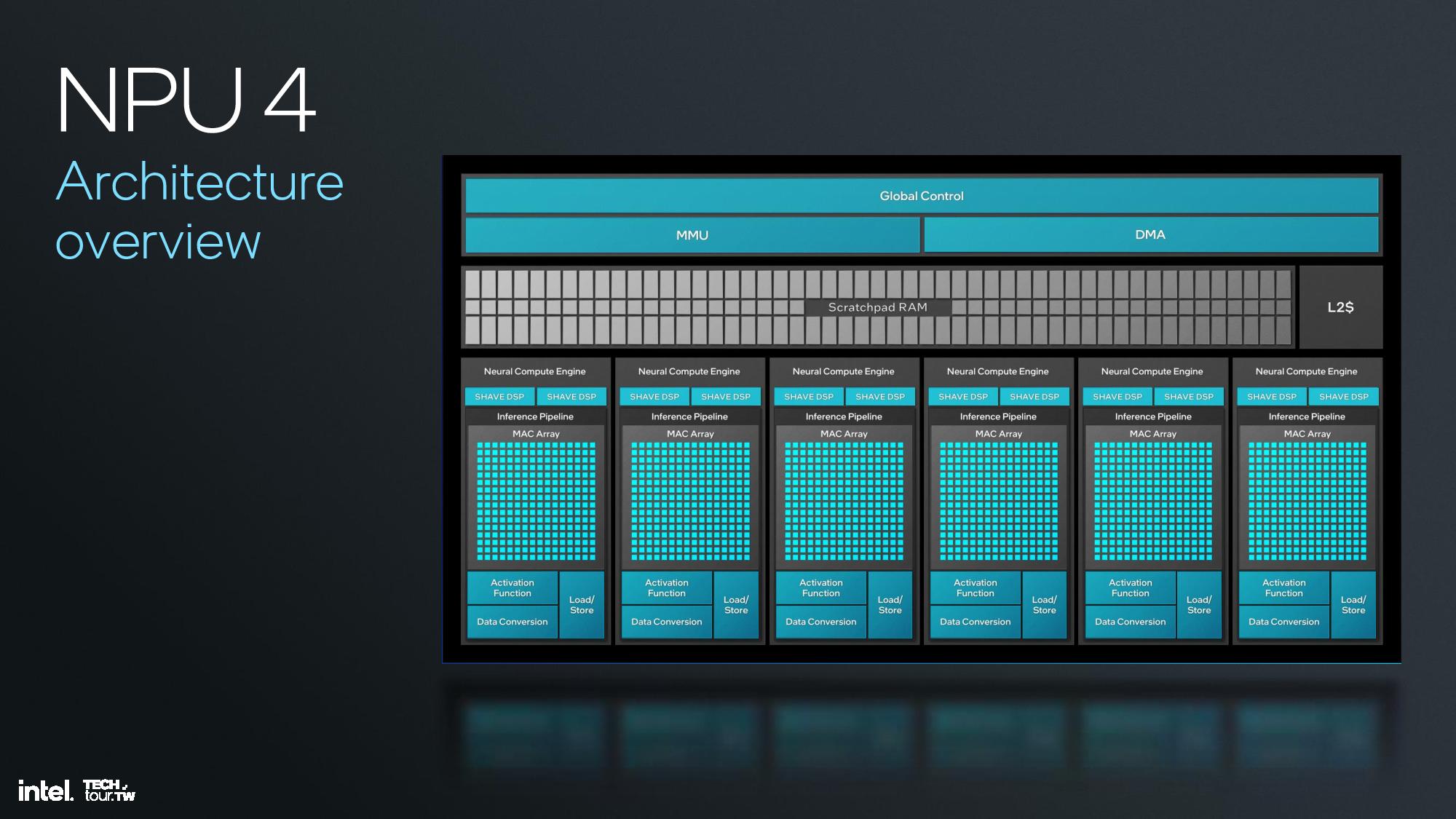
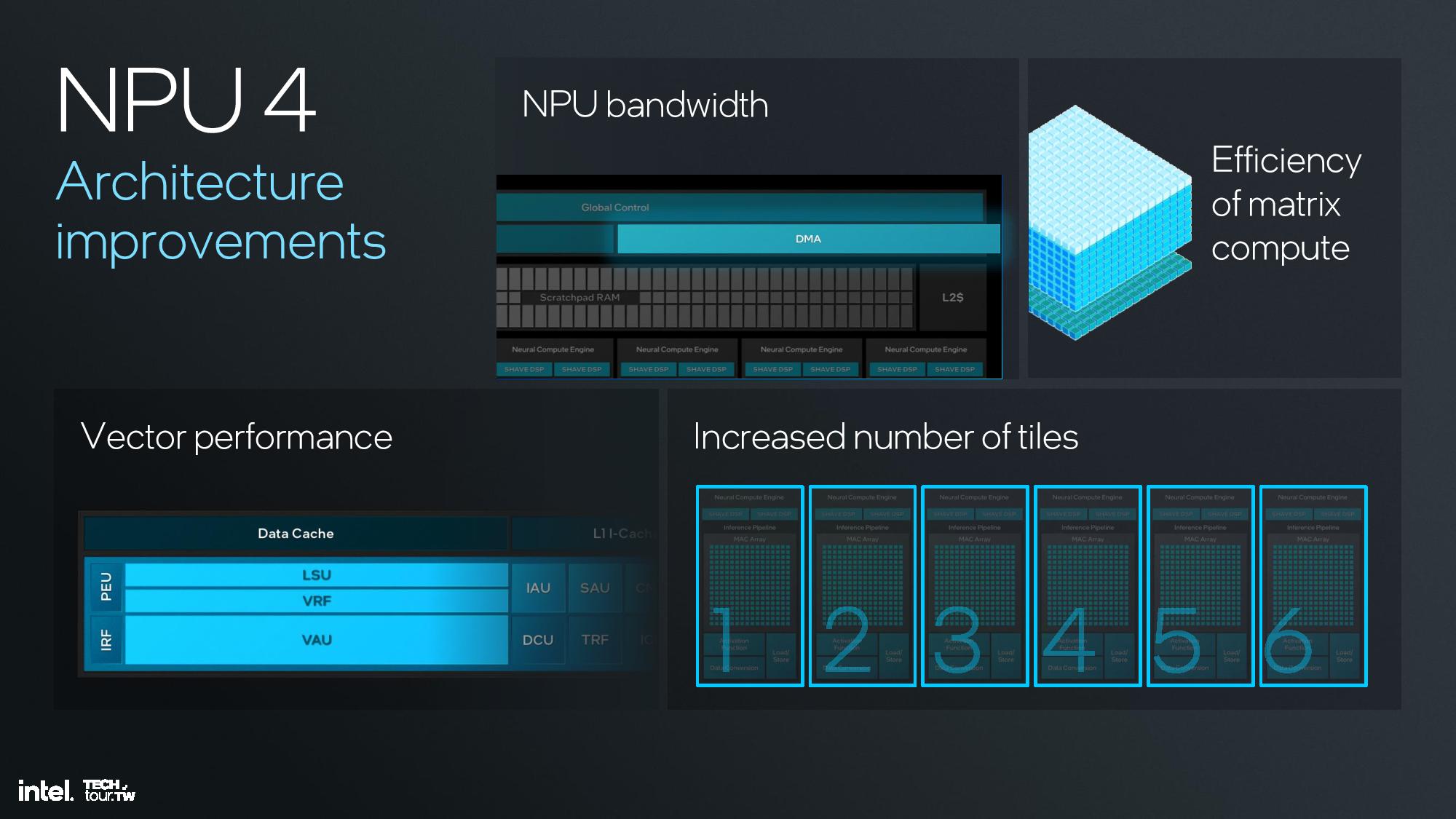
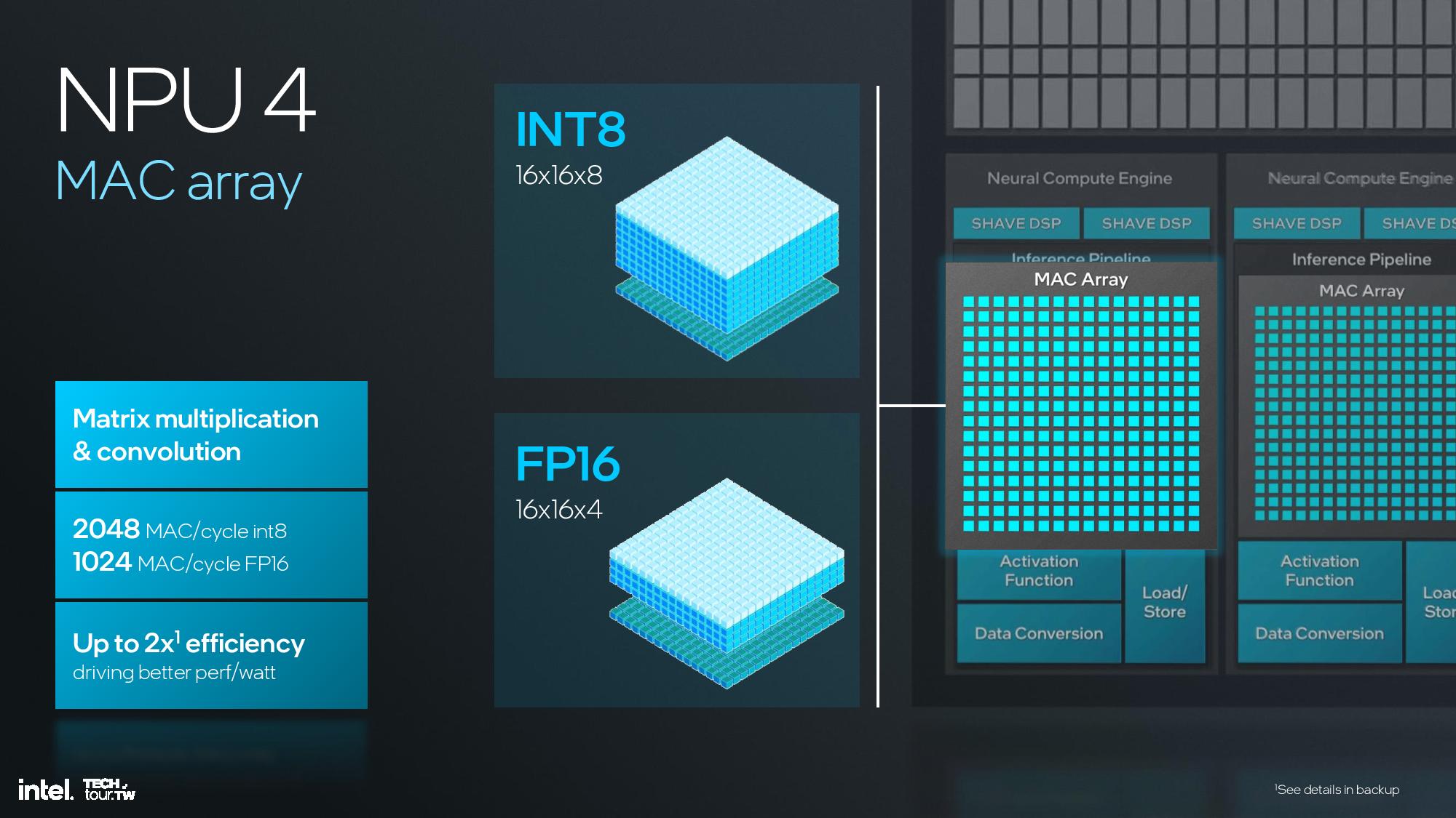
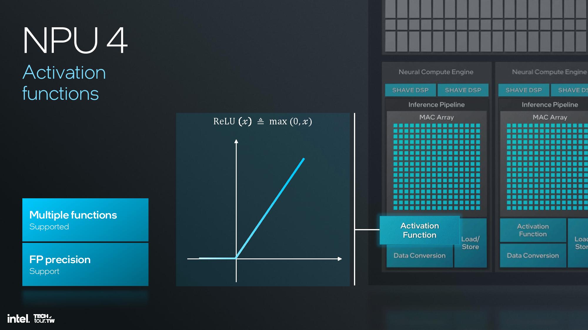
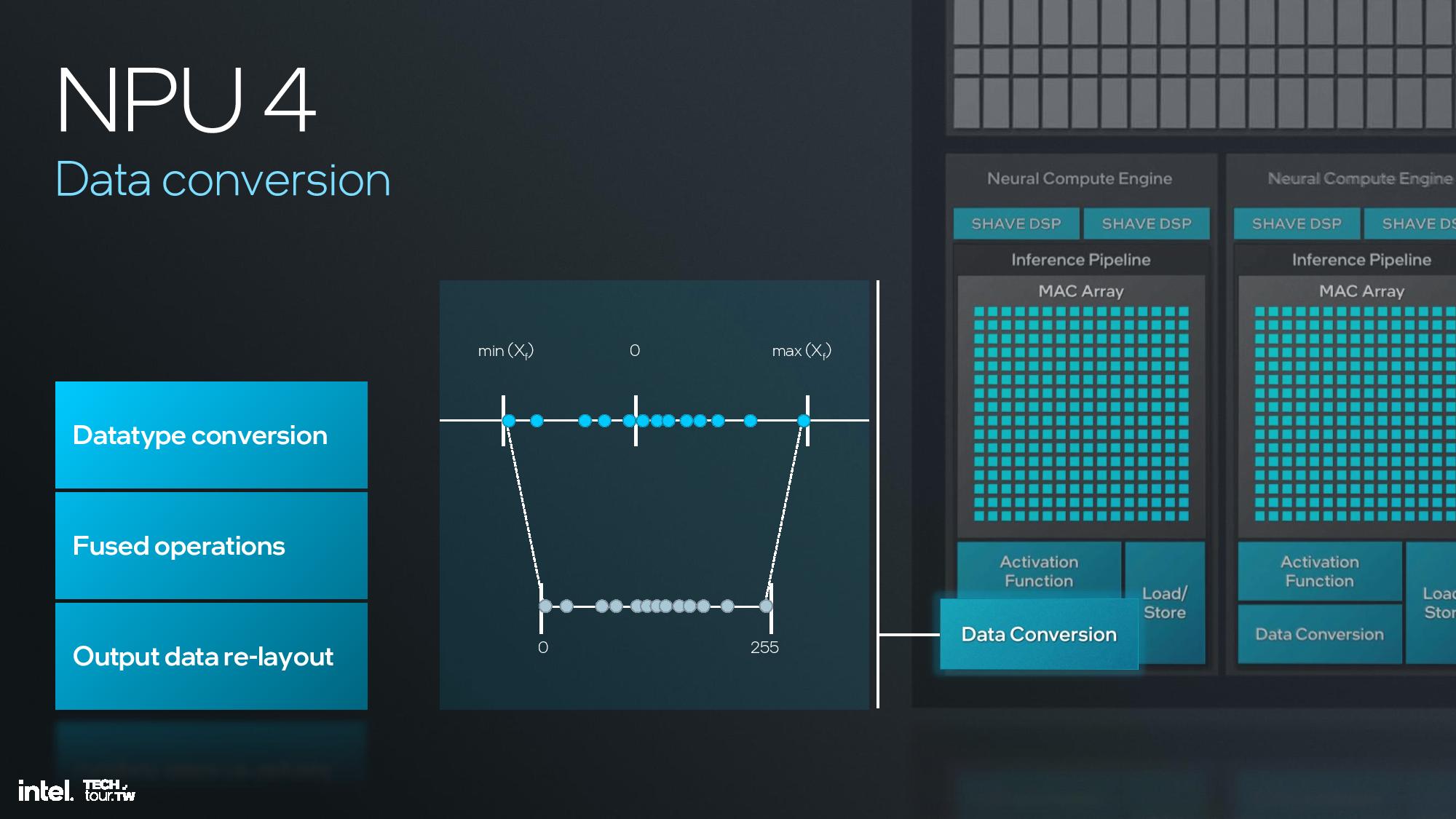
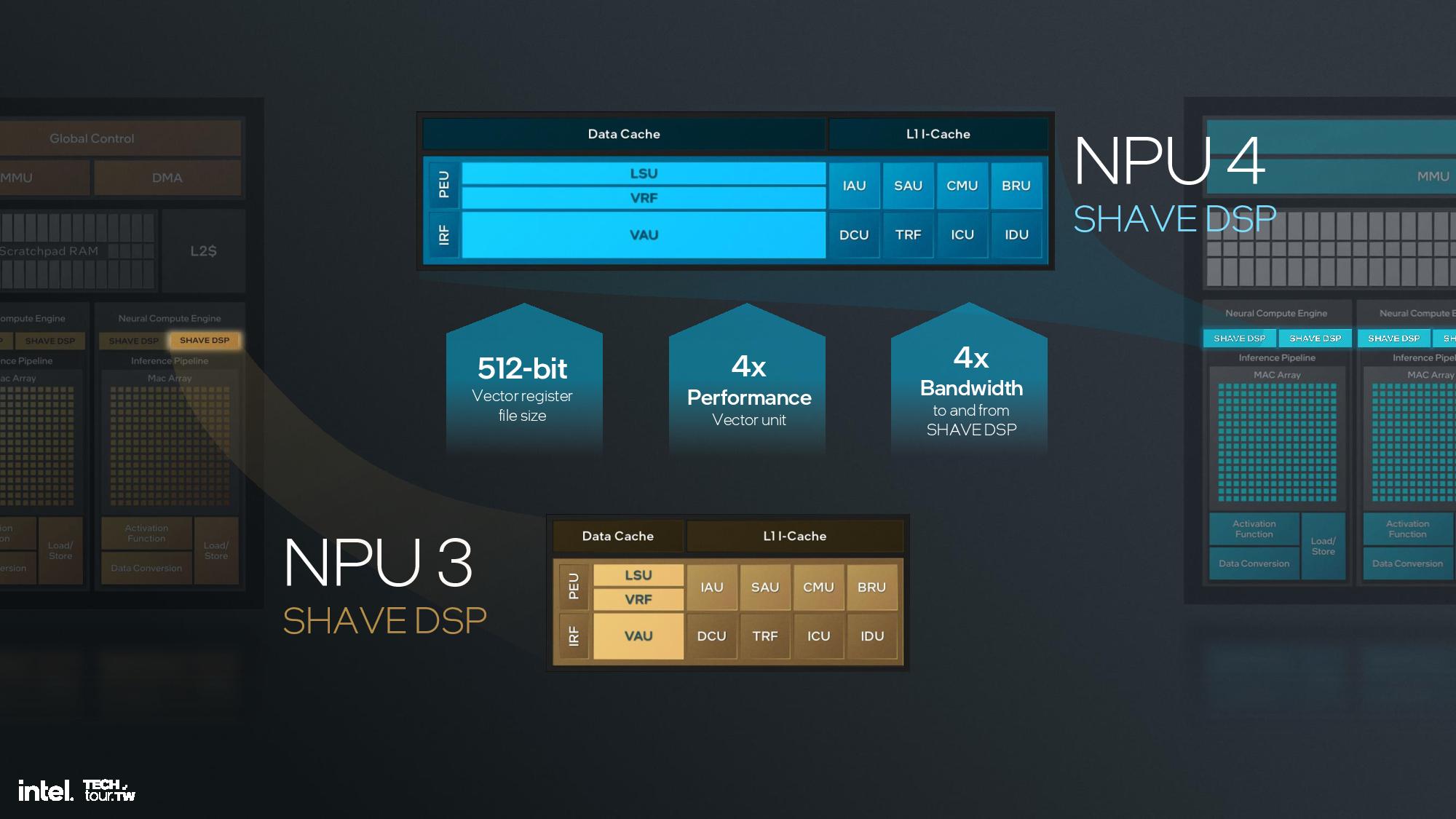
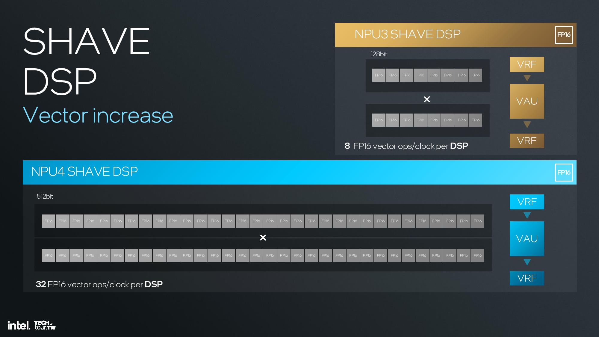
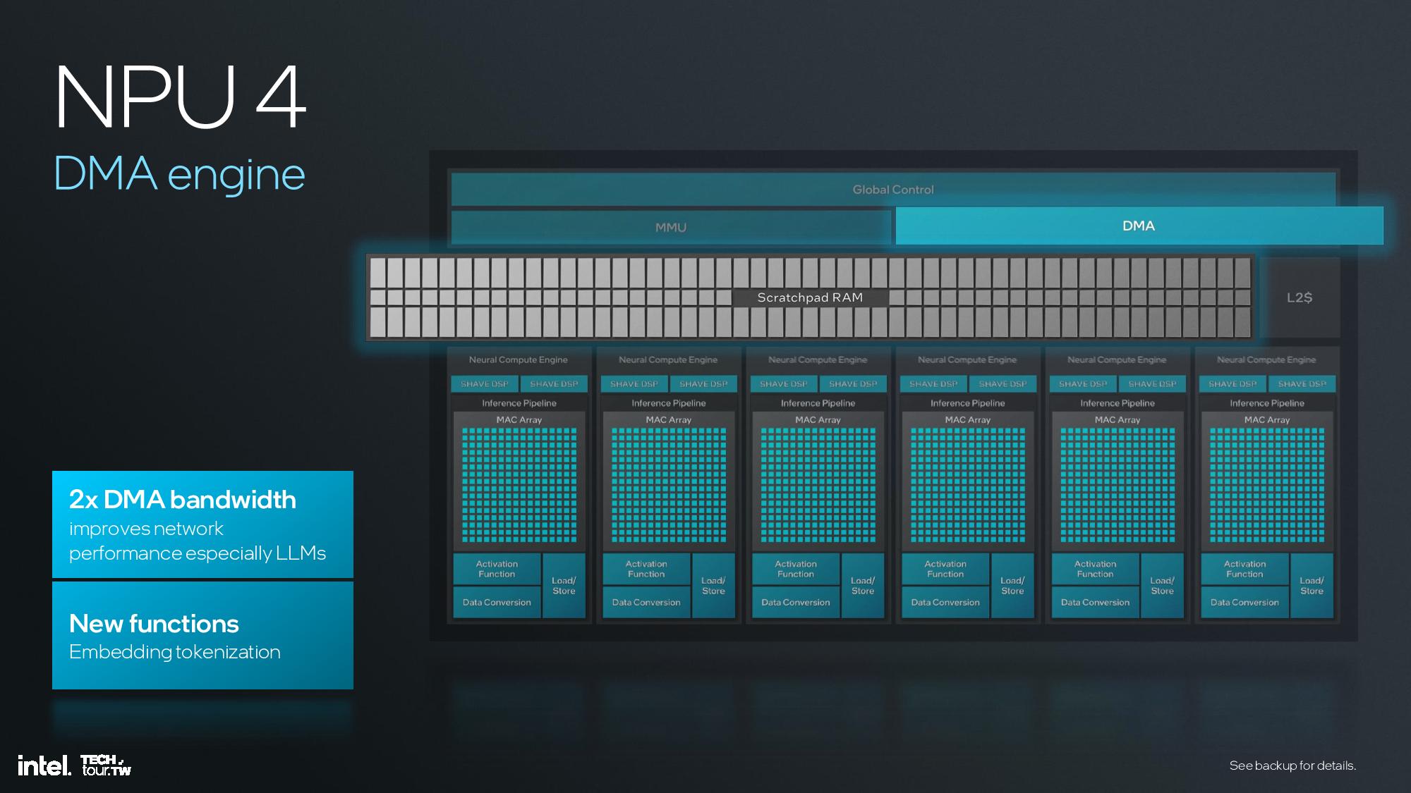
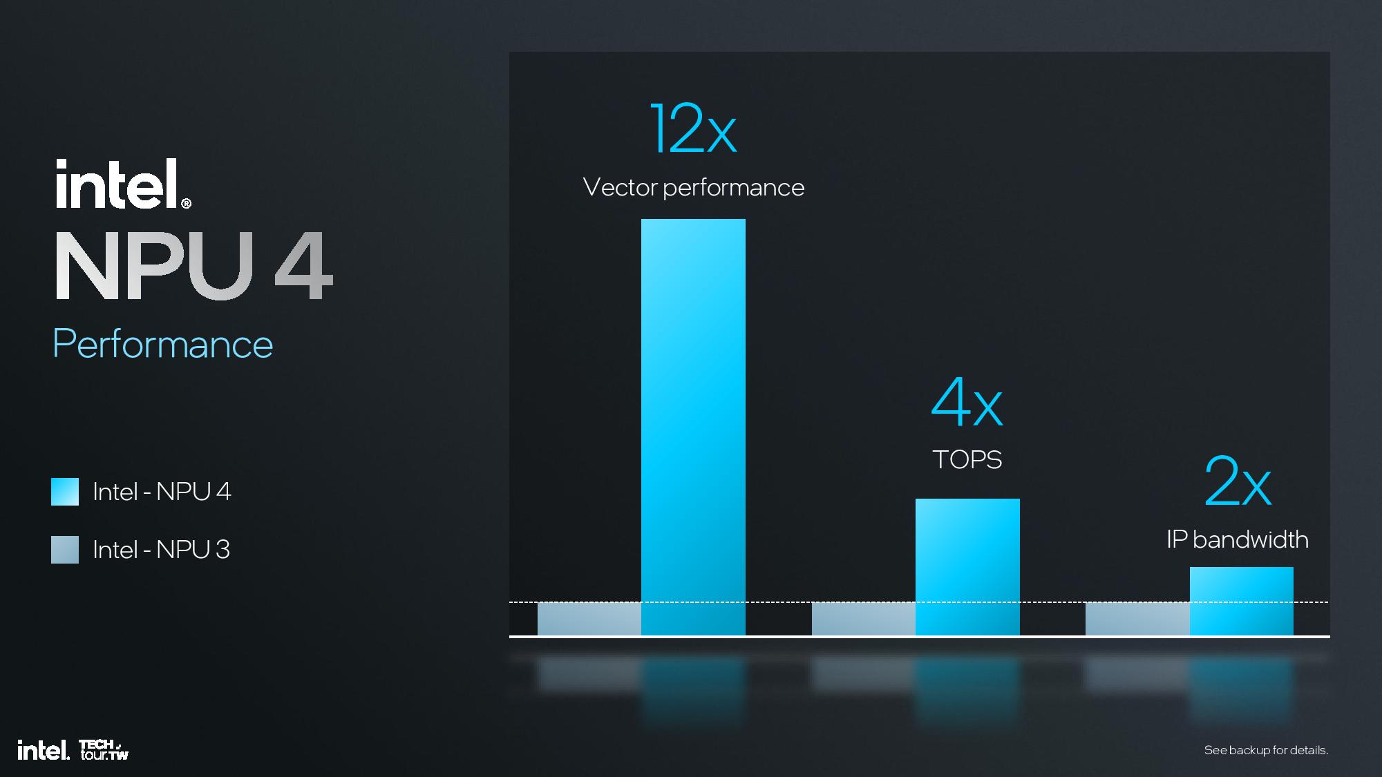
The key architectural components include 12 enhanced SHAVE DSPs, six neural compute engines, and a MAC array and DMA engine. This is fed with twice the memory bandwidth of the prior-gen NPU on Meteor Lake, and the NPU also has access to the 8MB shared side cache on the compute tile. This further enhances efficiency.
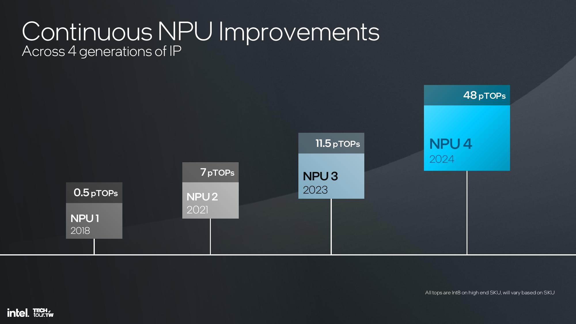
Overall Intel claims a 4X improvement in peak performance and a 2X improvement in performance at the same power over the previous-gen NPU 3.0 used in Meteor Lake.
Lunar Lake Platform Controller Tile and Connectivity
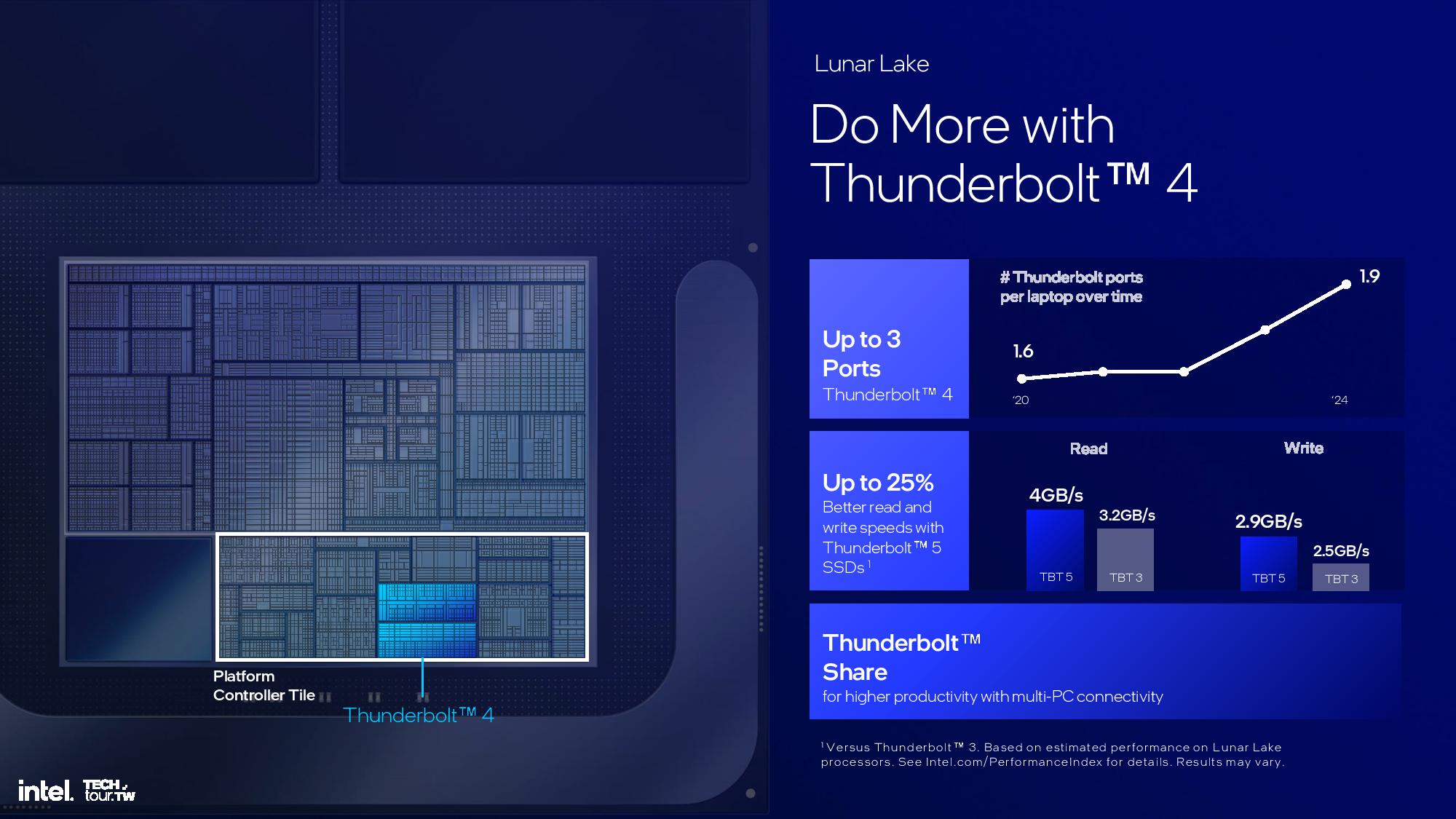
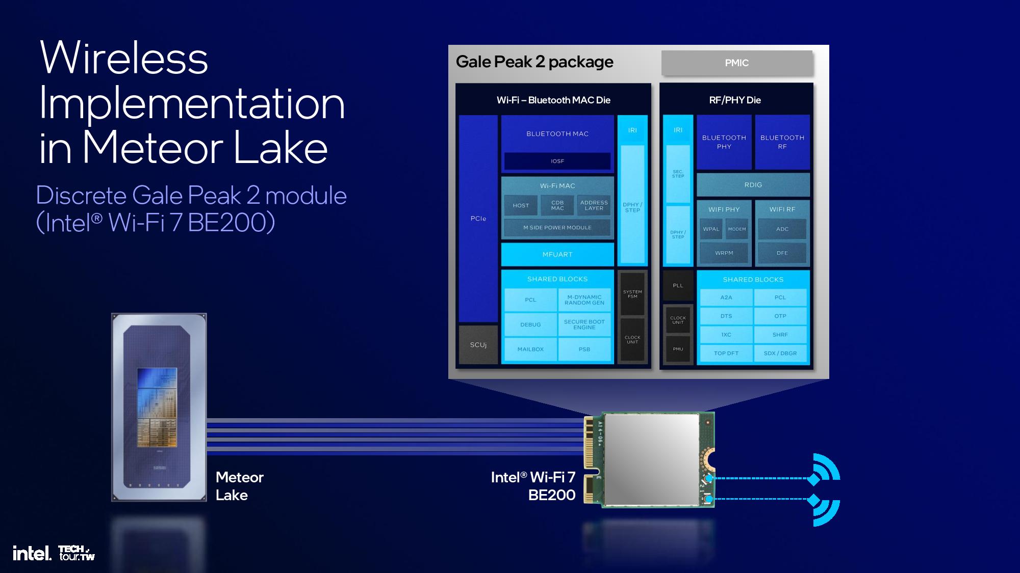
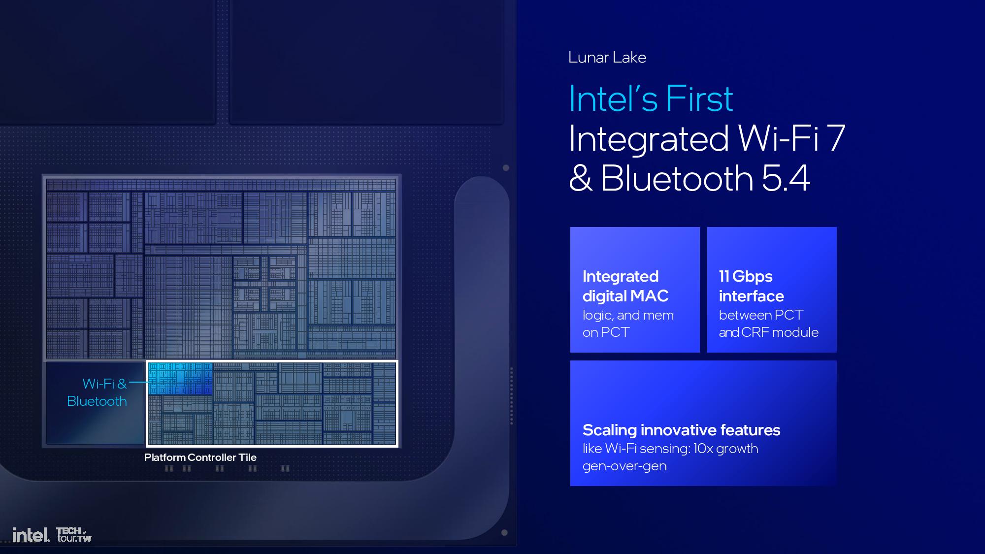
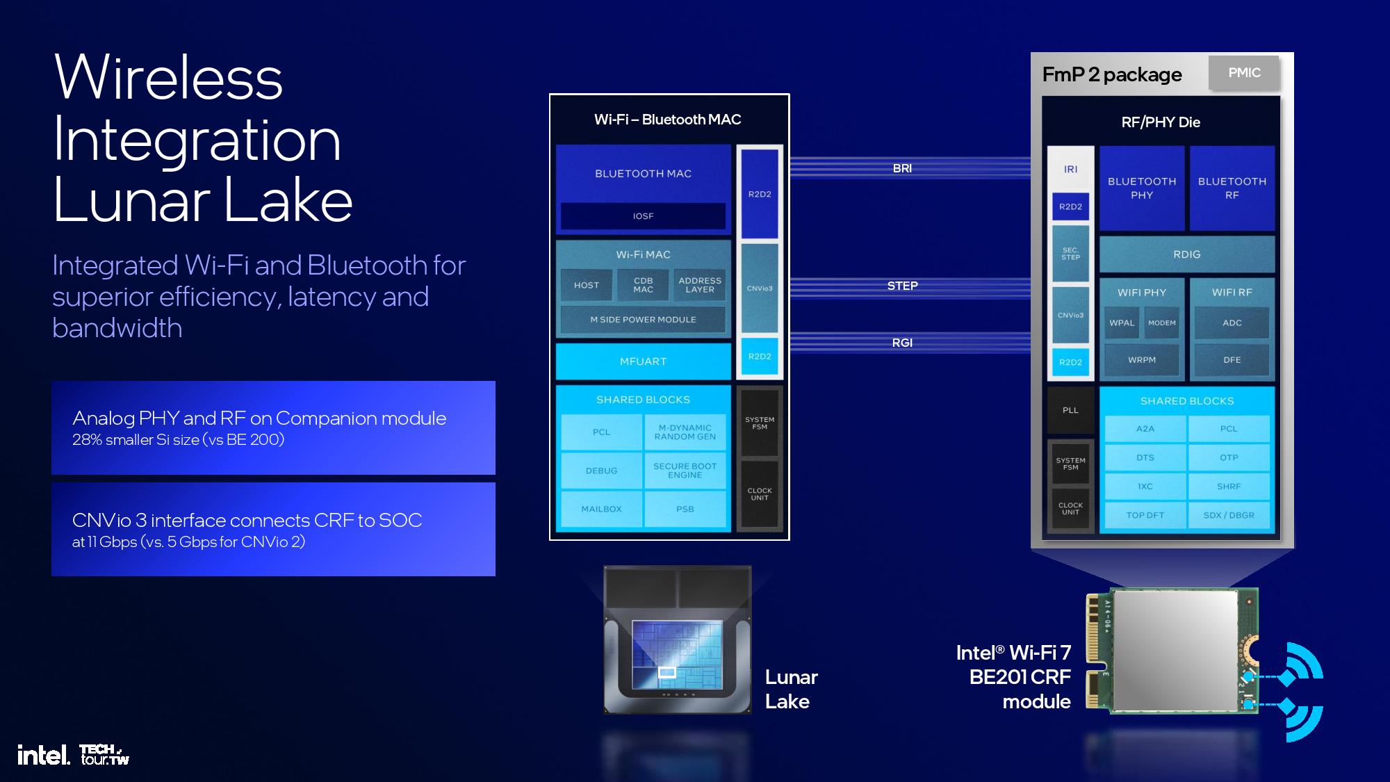
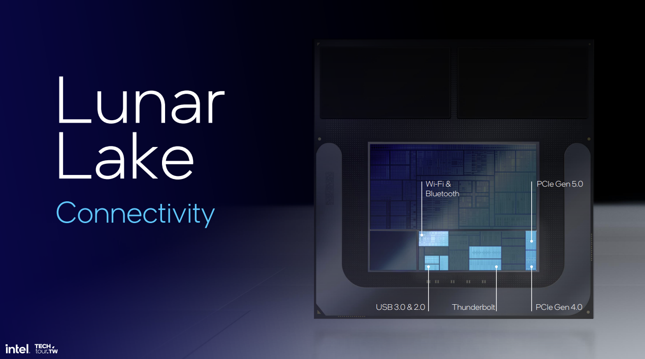
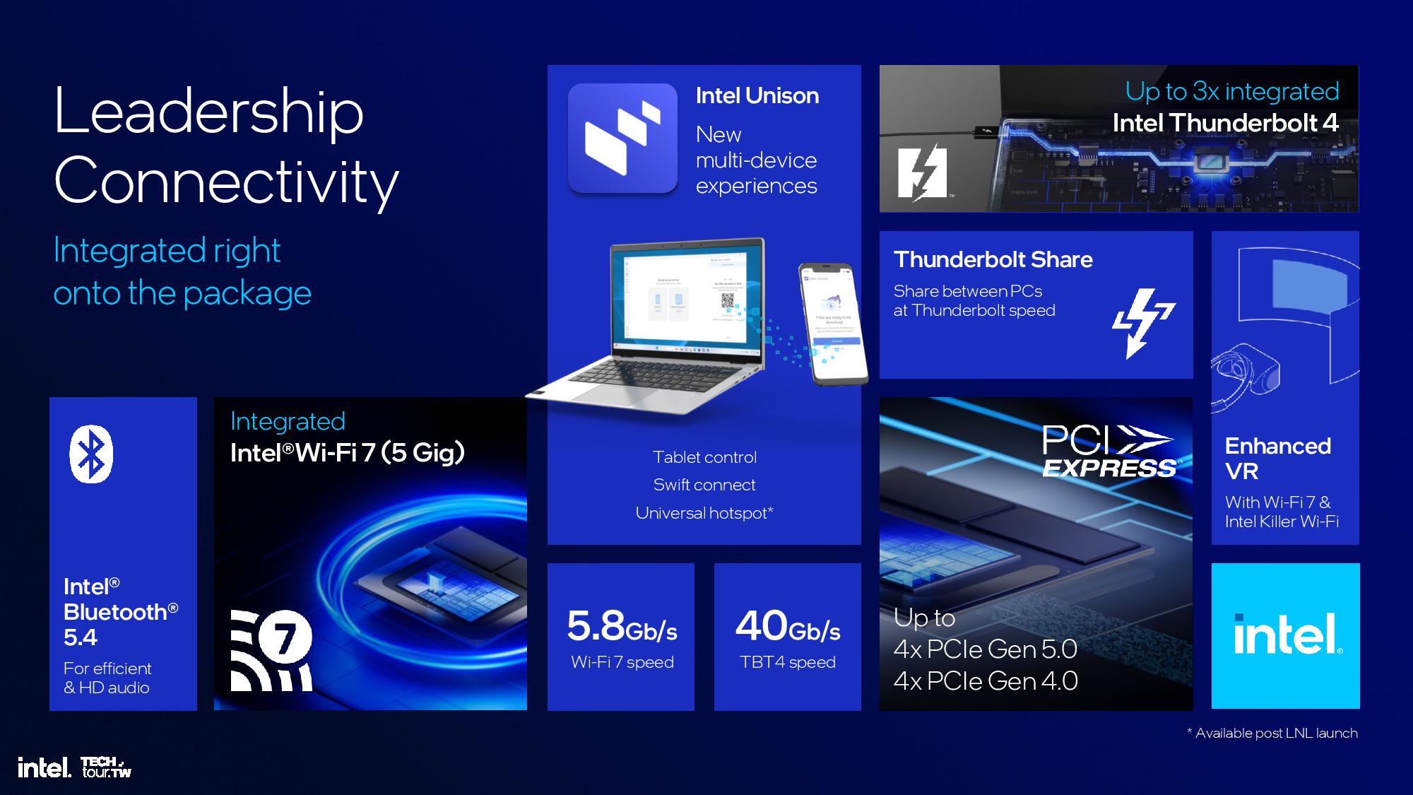
The Platform Controller Tile houses all of the external I/O functions for the chip, including Wi-Fi and Bluetooth, USB 3.0 and 2. 0, Thunderbolt, and the PCIe 4.0 and 5.0 interfaces. It also houses the memory controllers.
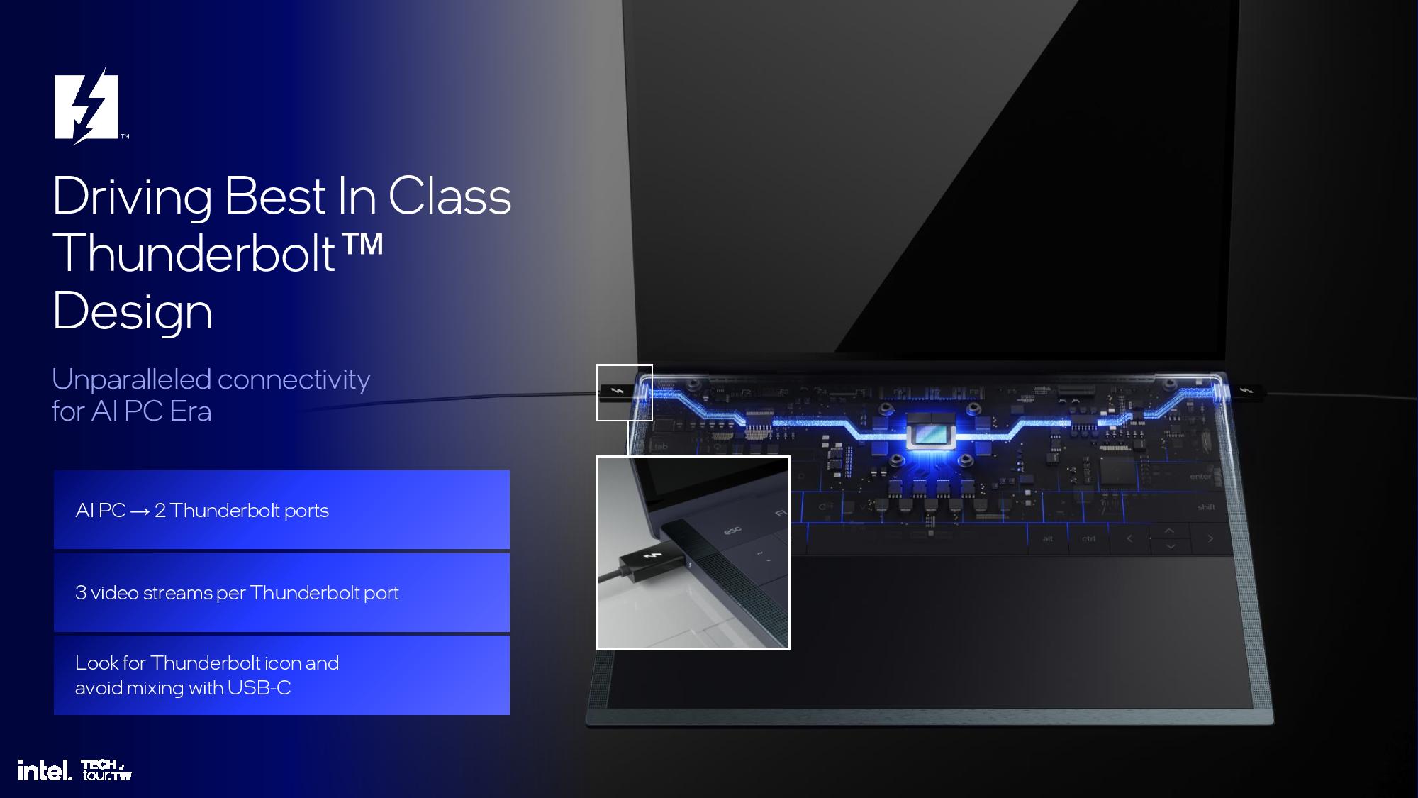
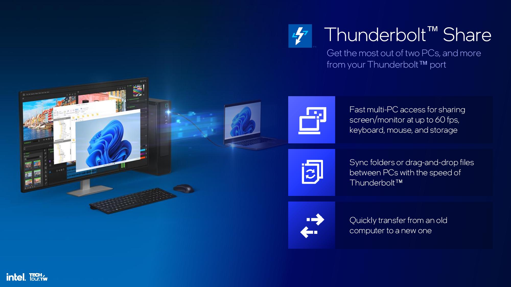
Intel guarantees that all Lunar Lake laptops will have at least two ports of Thunderbolt 4 connectivity, while some models will offer up to three ports. Intel used Thunderbolt 4 instead of the newer Thunderbolt 5 due to the target market for this class of laptop. The interface also supports the new Thunderbolt Share feature, which allows the interface to provide drag-and-drop file sharing functionality between PCs, along with screen and peripheral sharing.
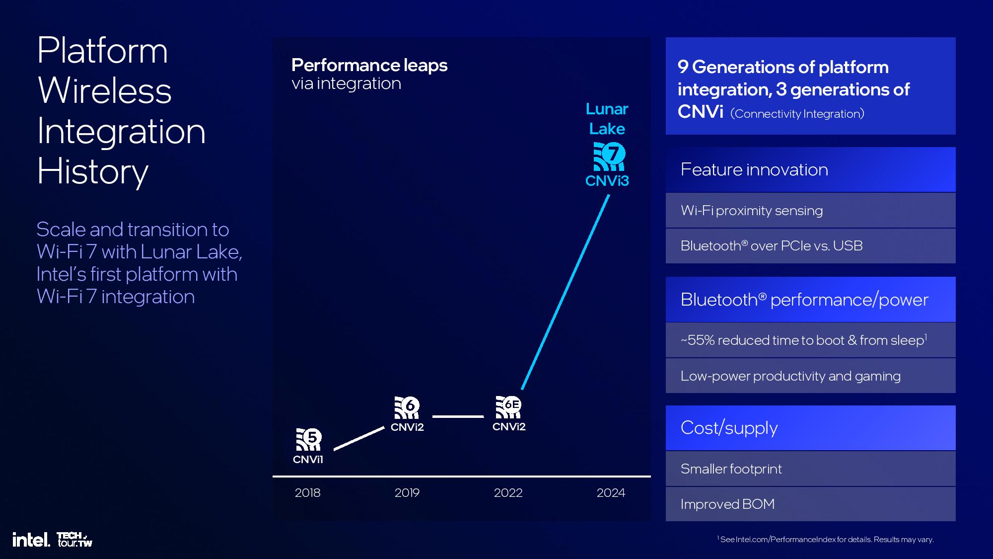
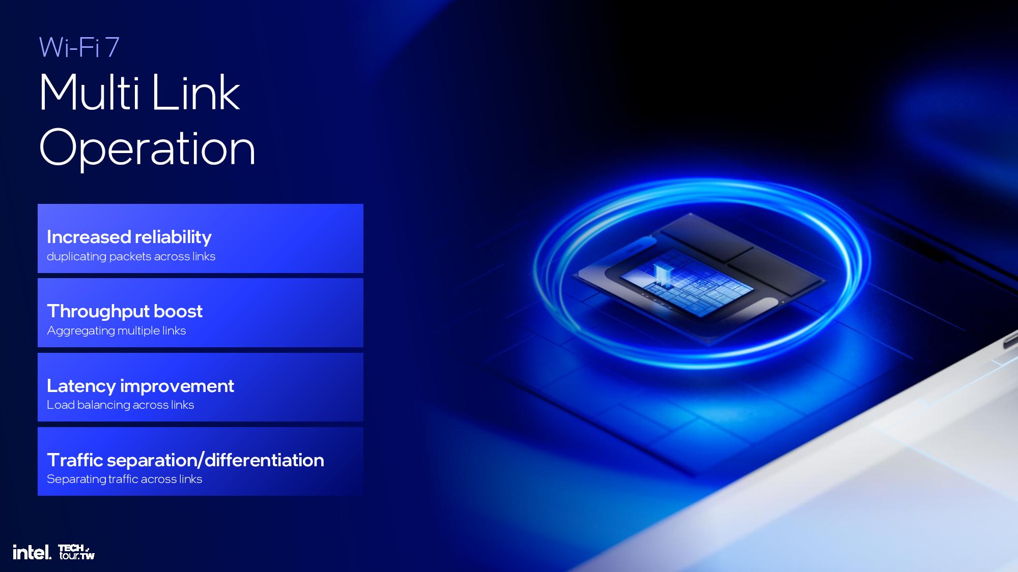
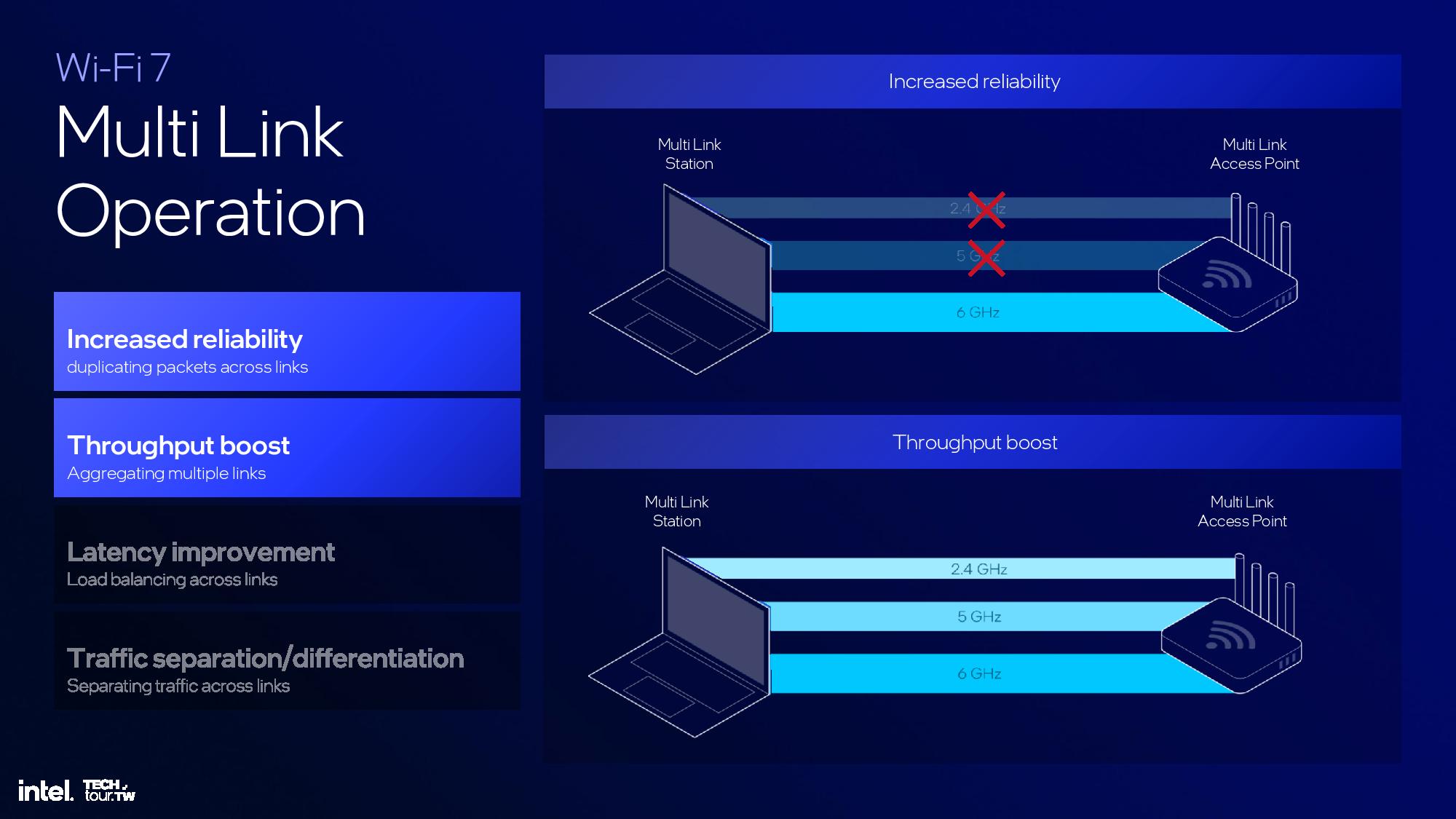
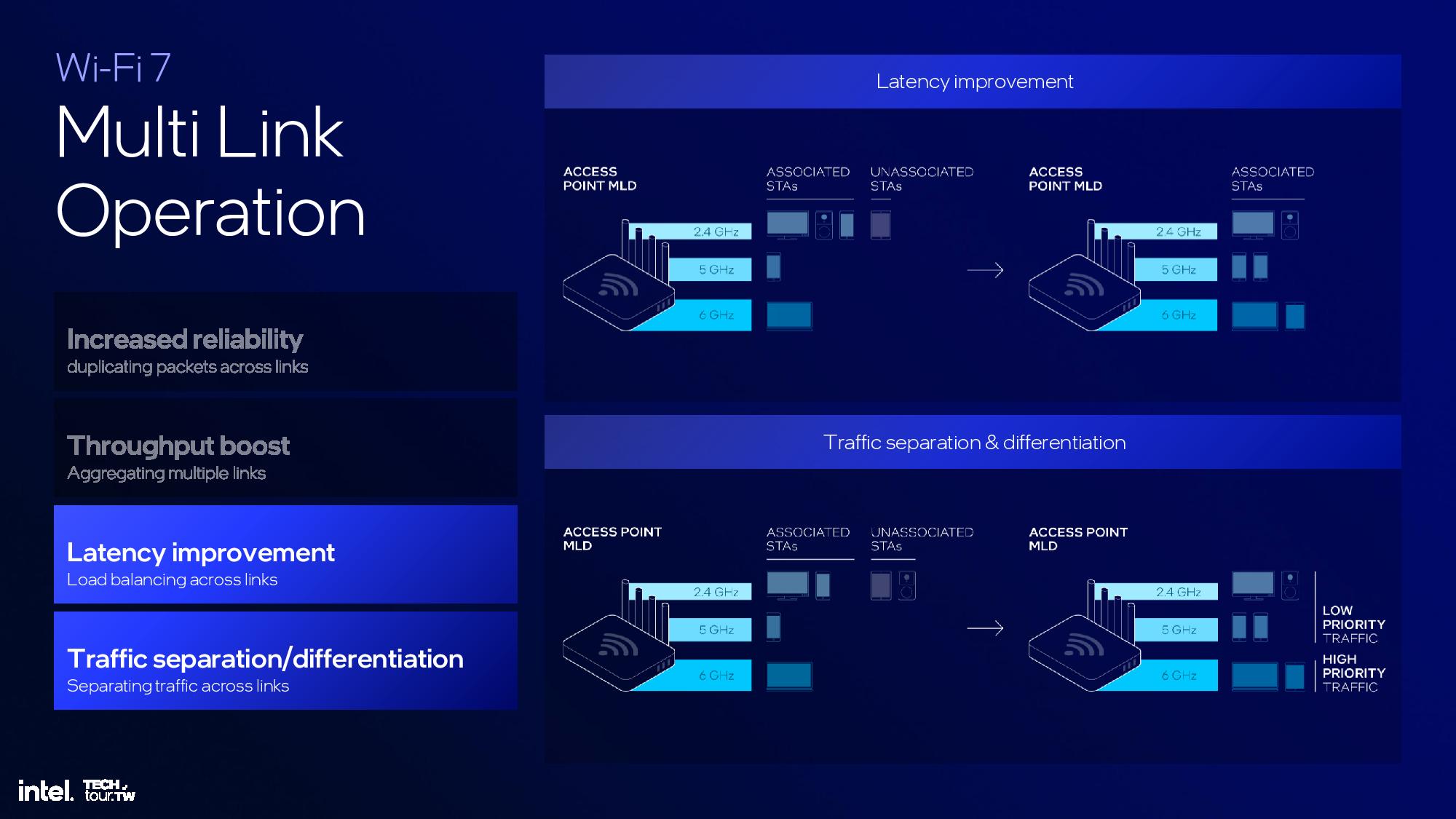
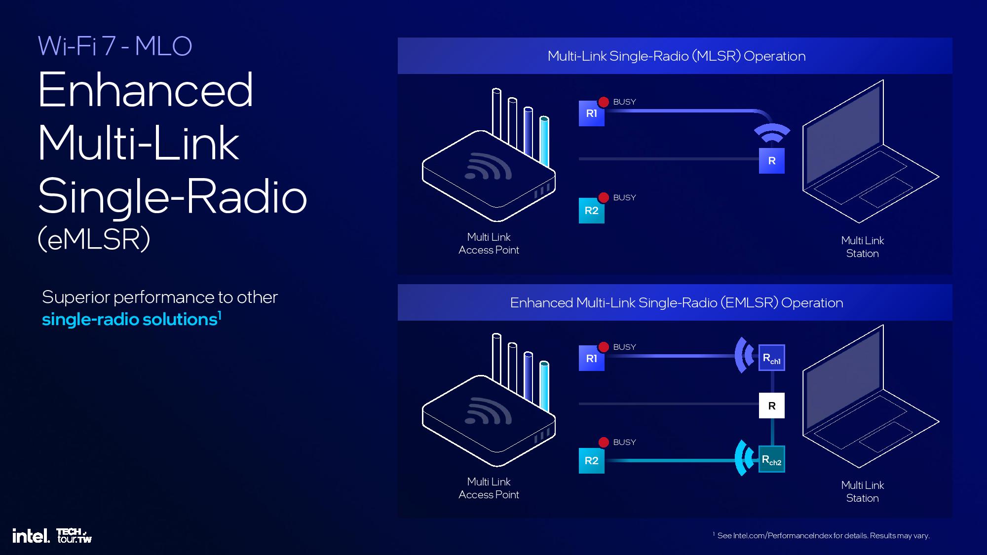
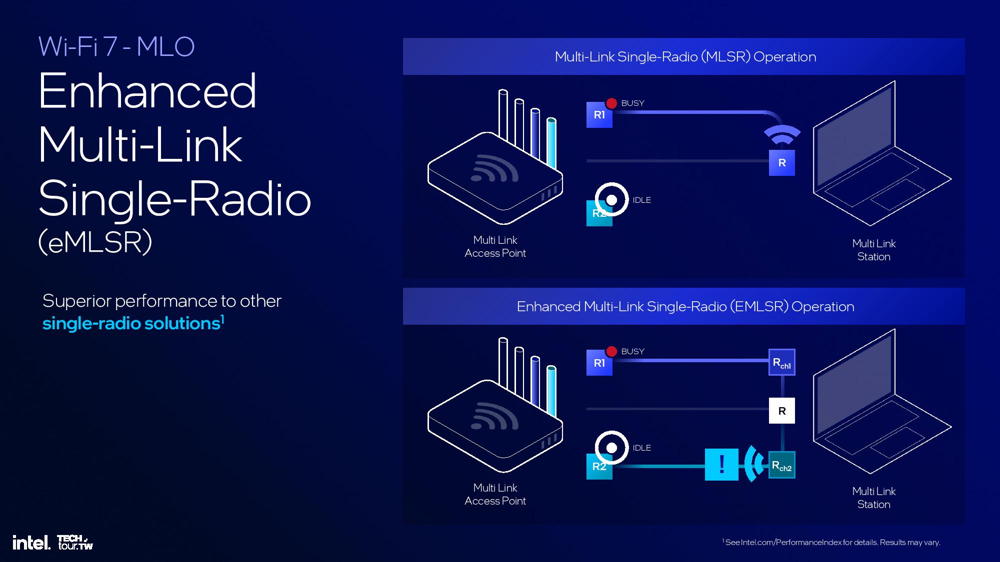
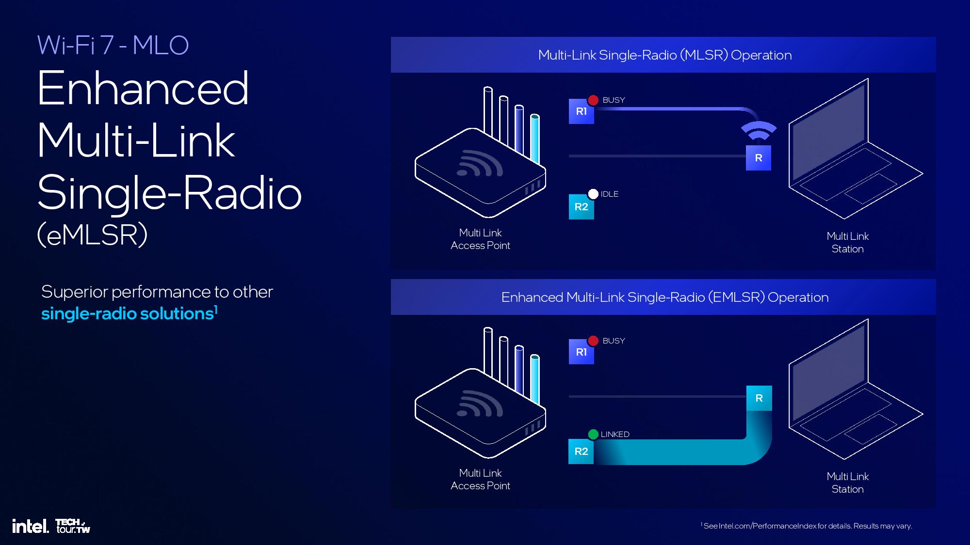
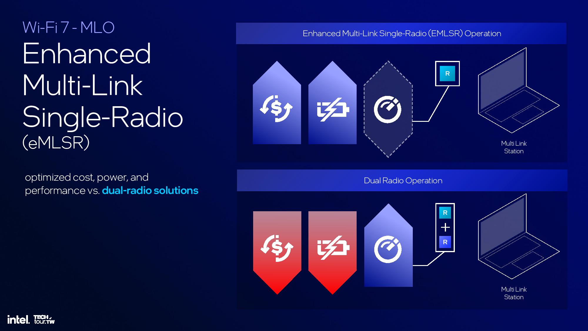
The platform also supports Bluetooth 5.4 and Wi-Fi 7 that’s partially embedded into the Platform Controller Tile. Wi-Fi 7 functionality still requires another CNVi module that’s connected externally via the CNVi 3.0 interface. The new BE201 CRF module is 28% smaller than prior-gen Wi-Fi modules.
Lunar Lake Thread Director Improvements

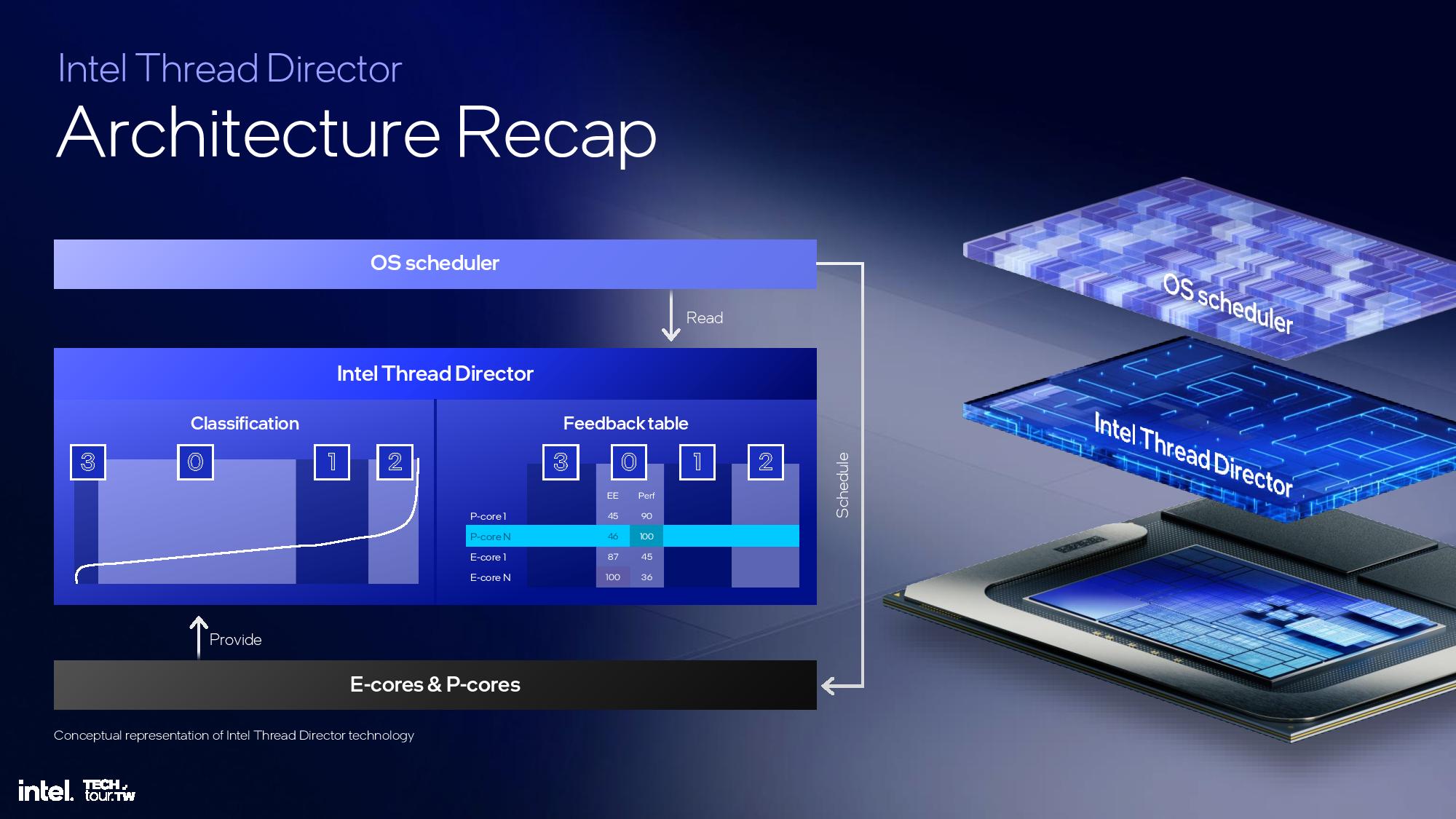
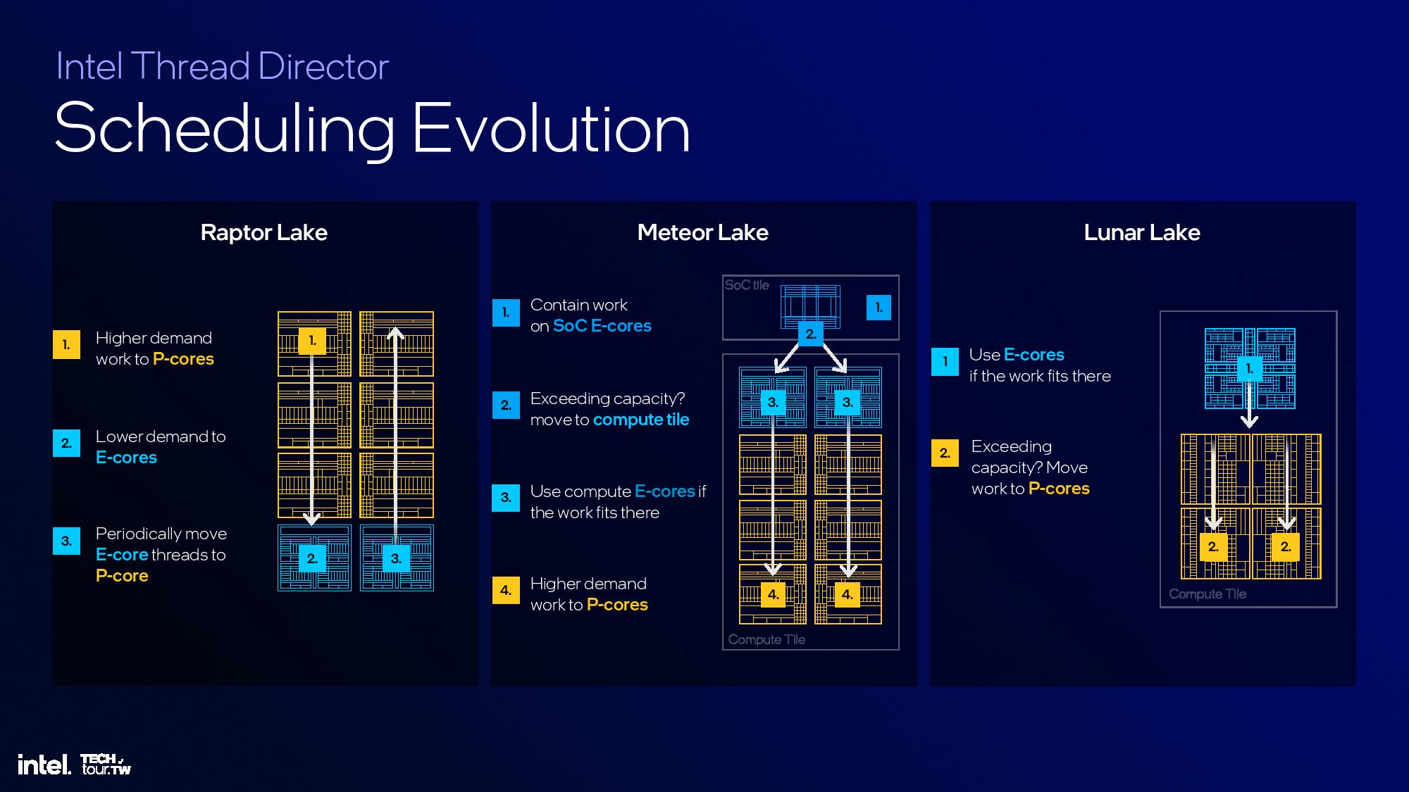
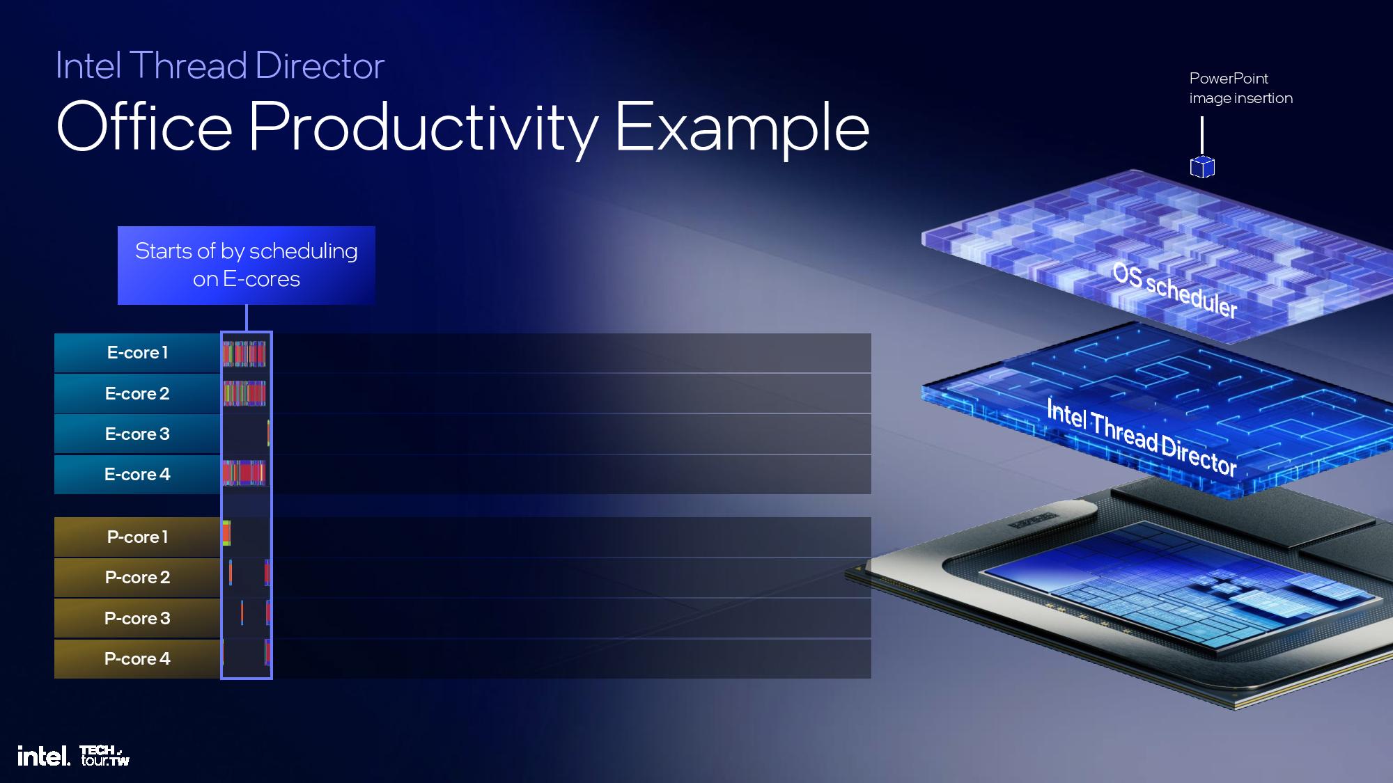
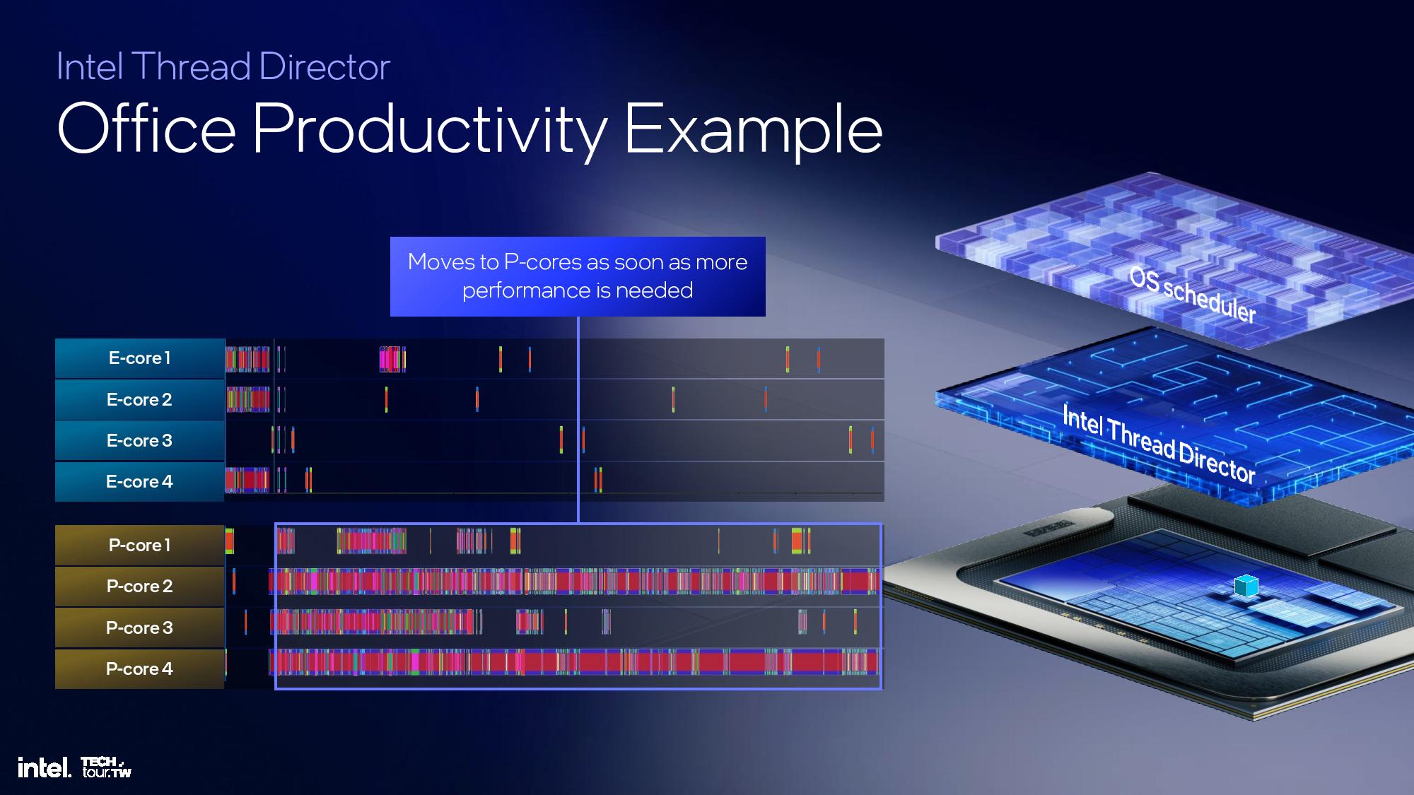
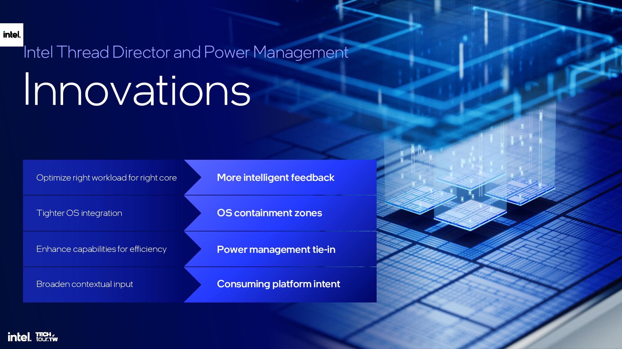
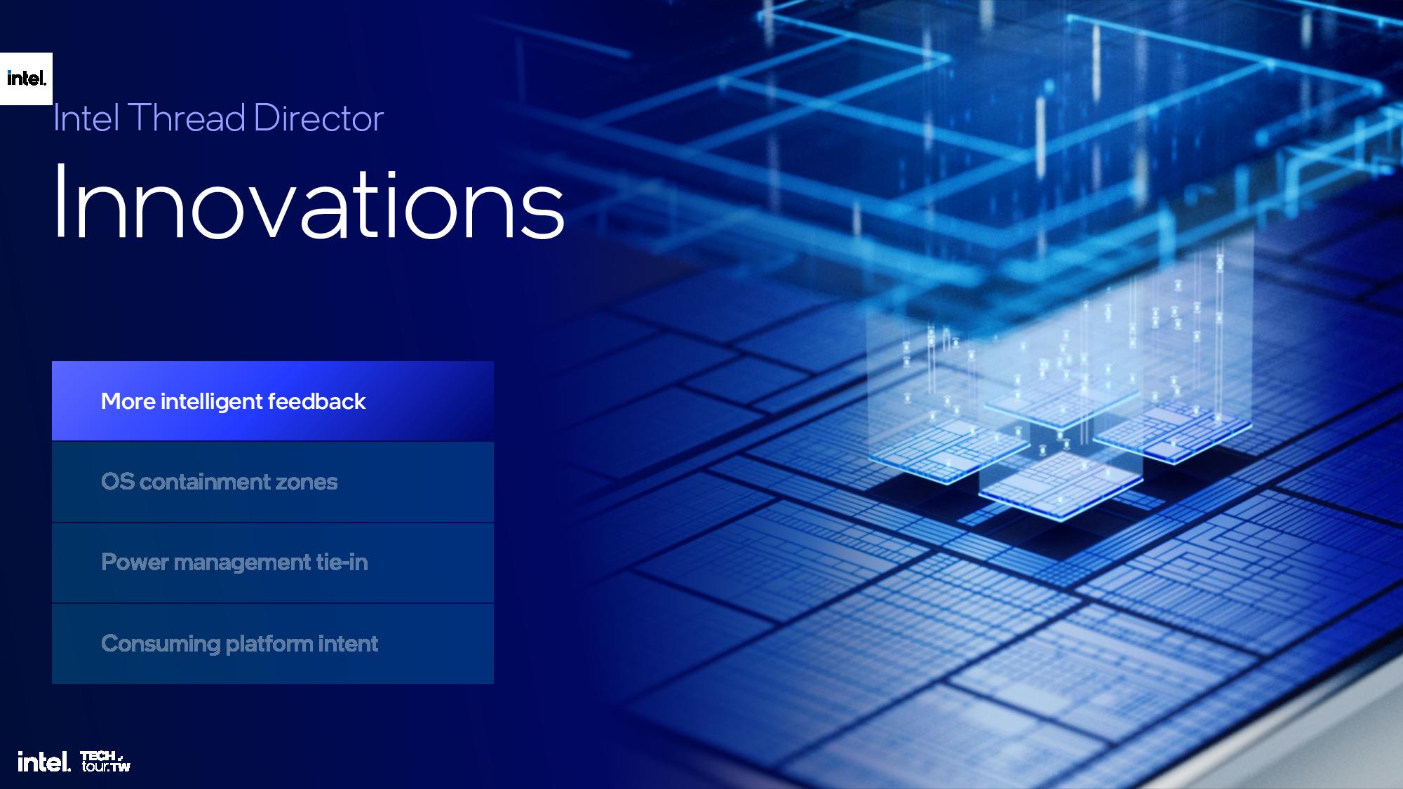
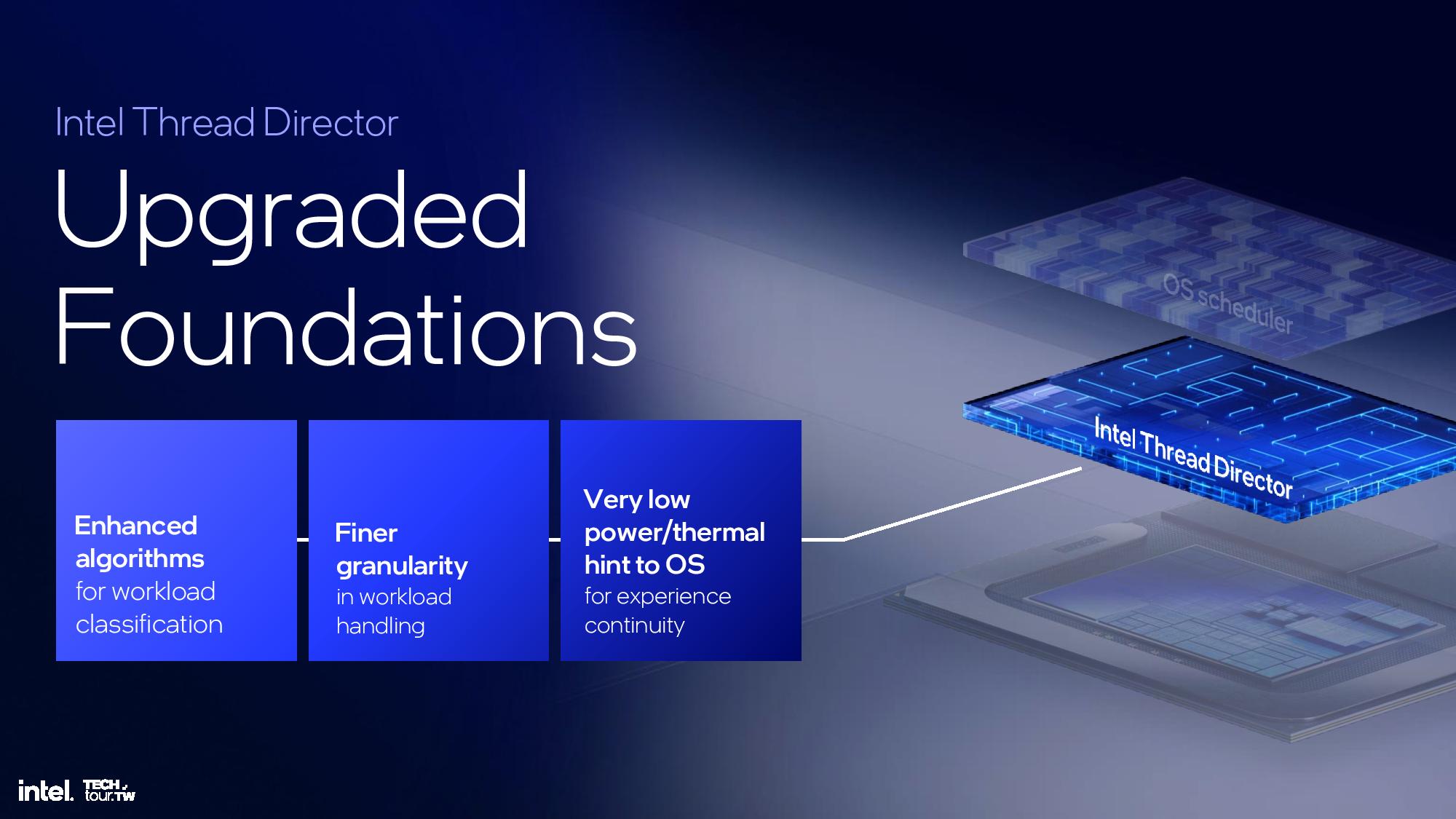
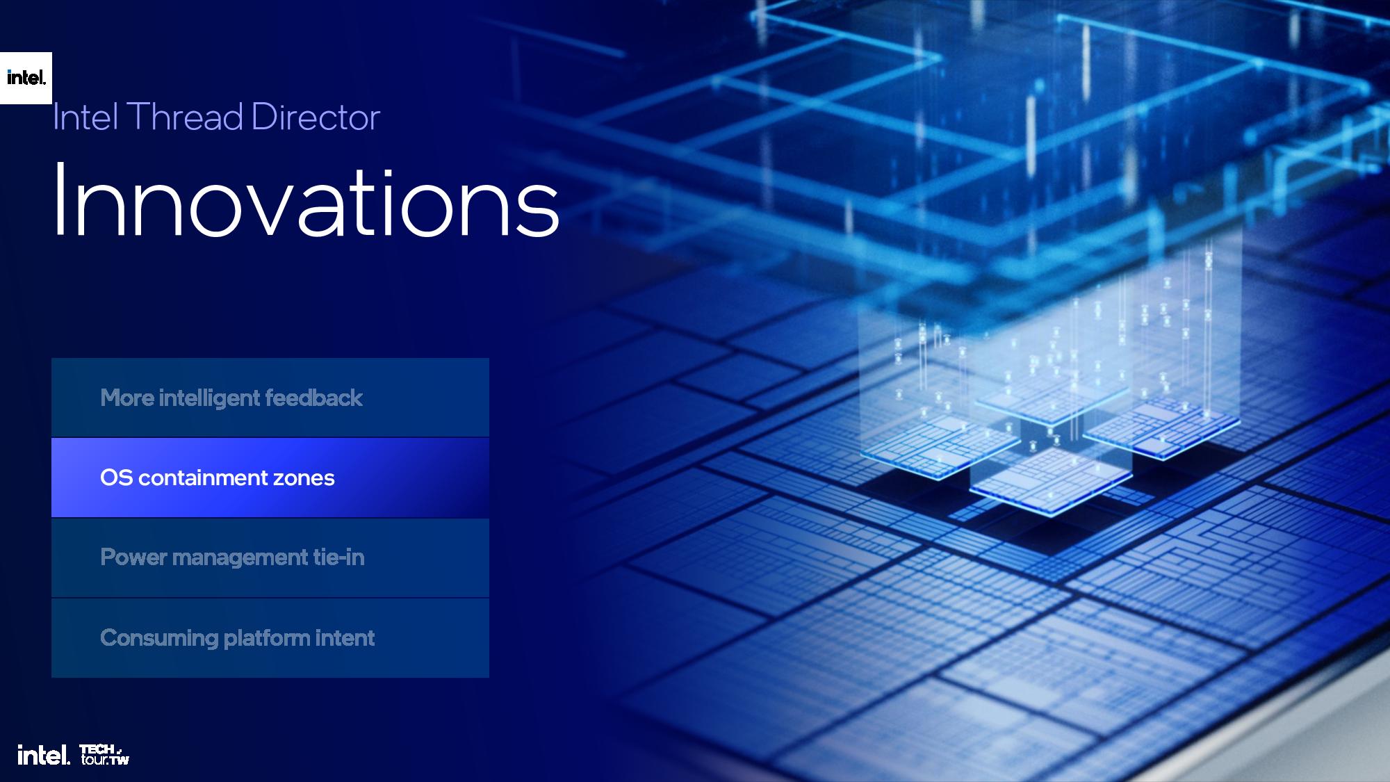
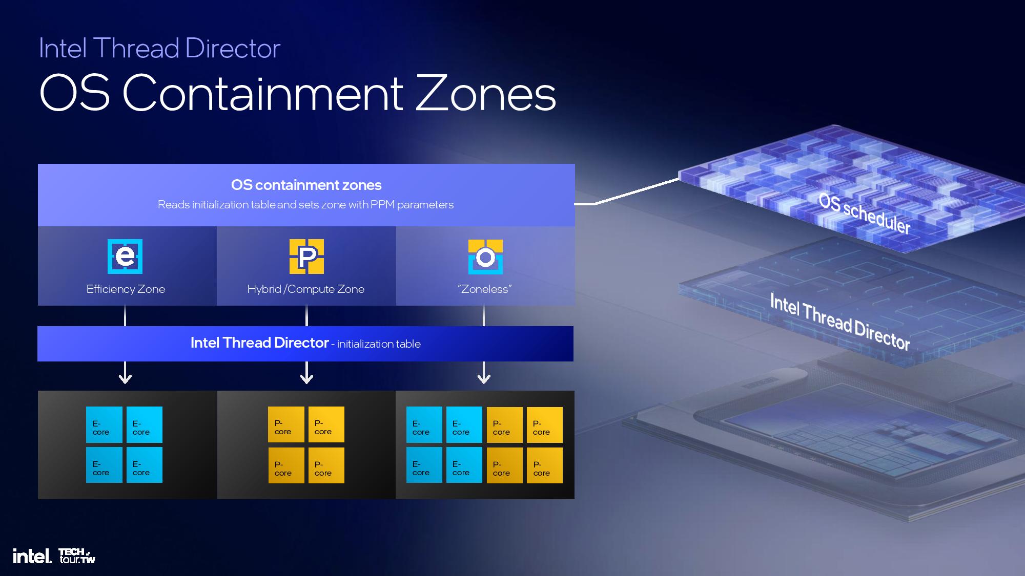
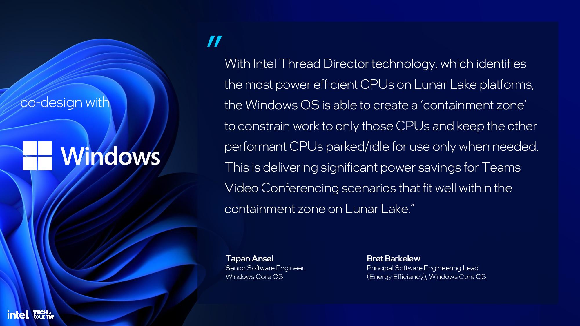
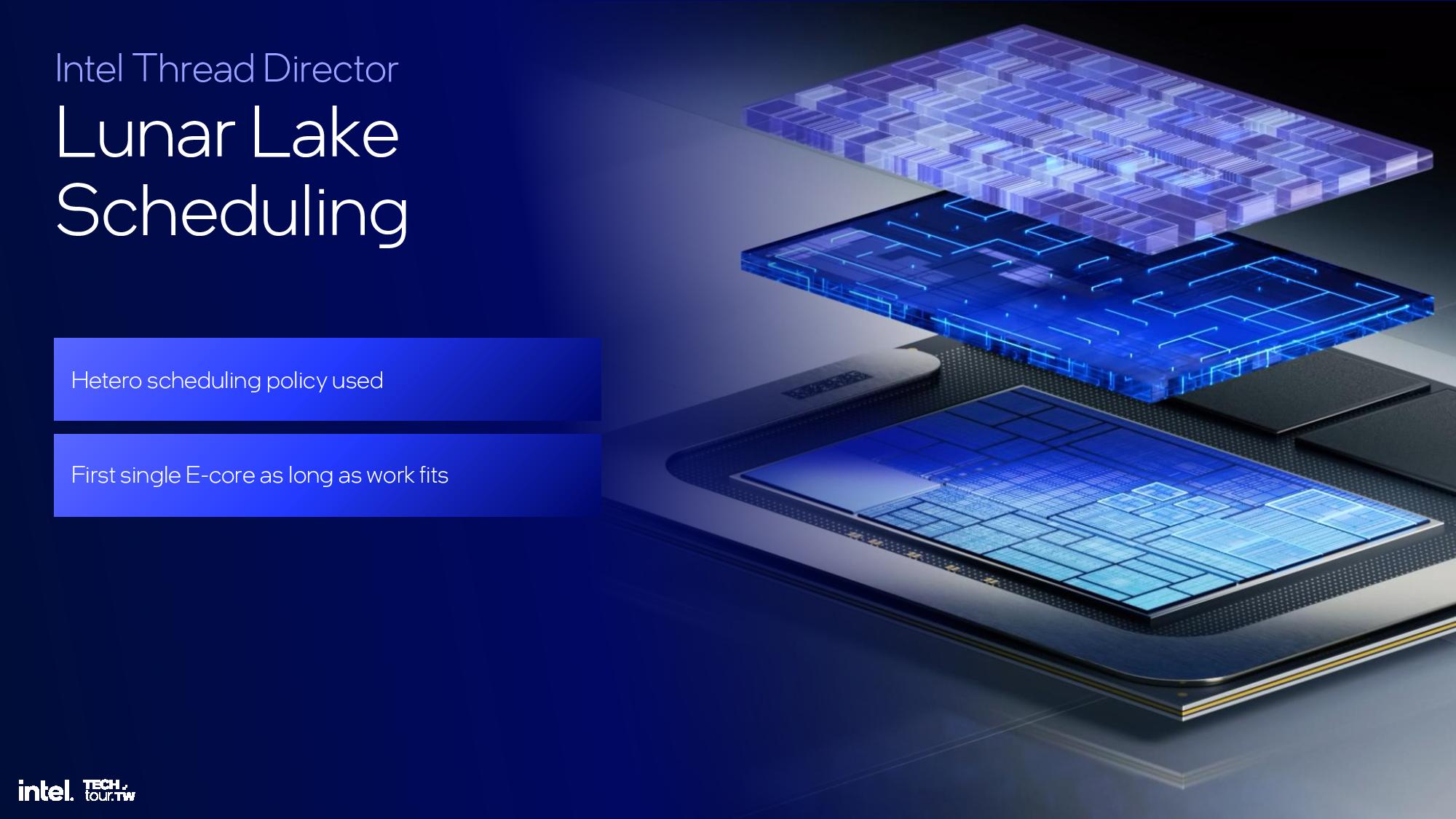
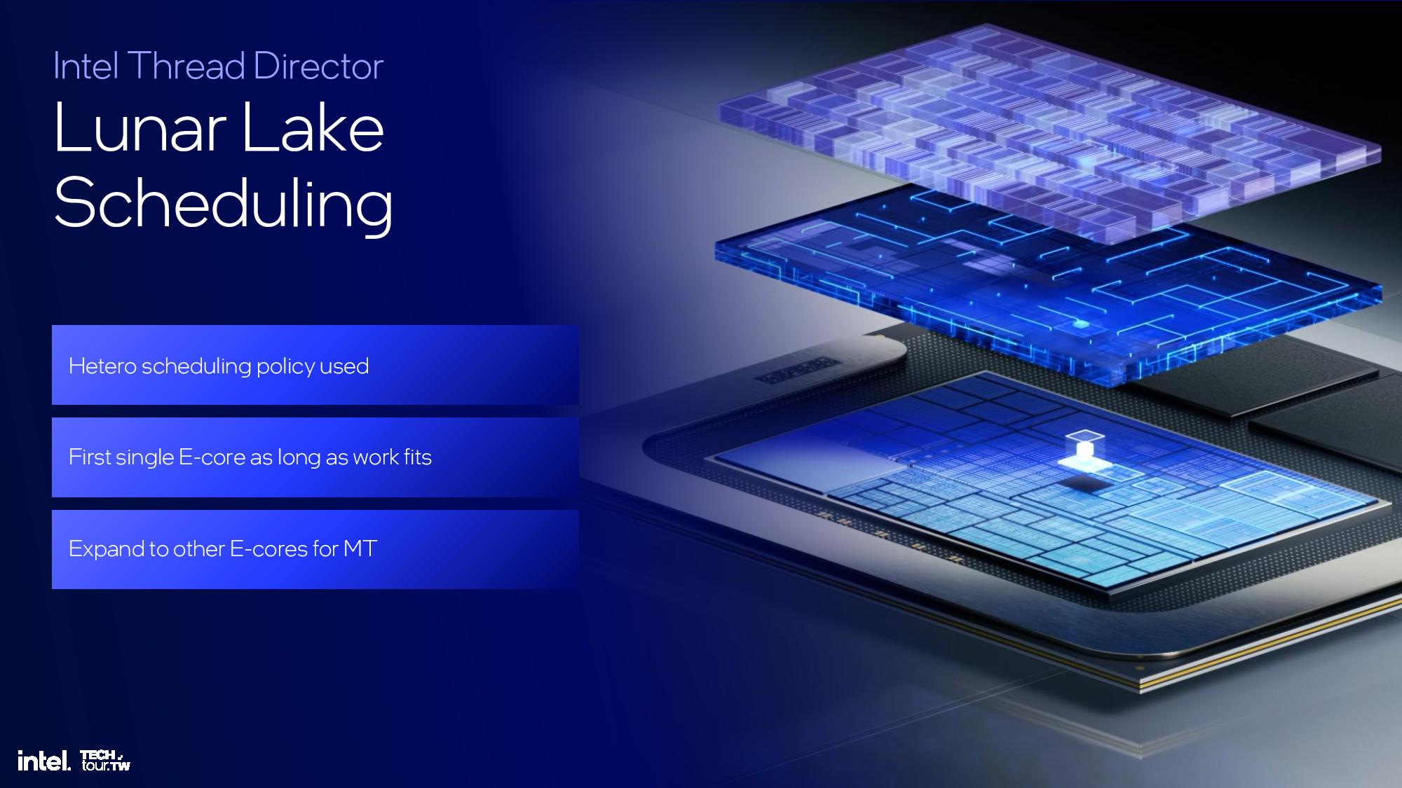
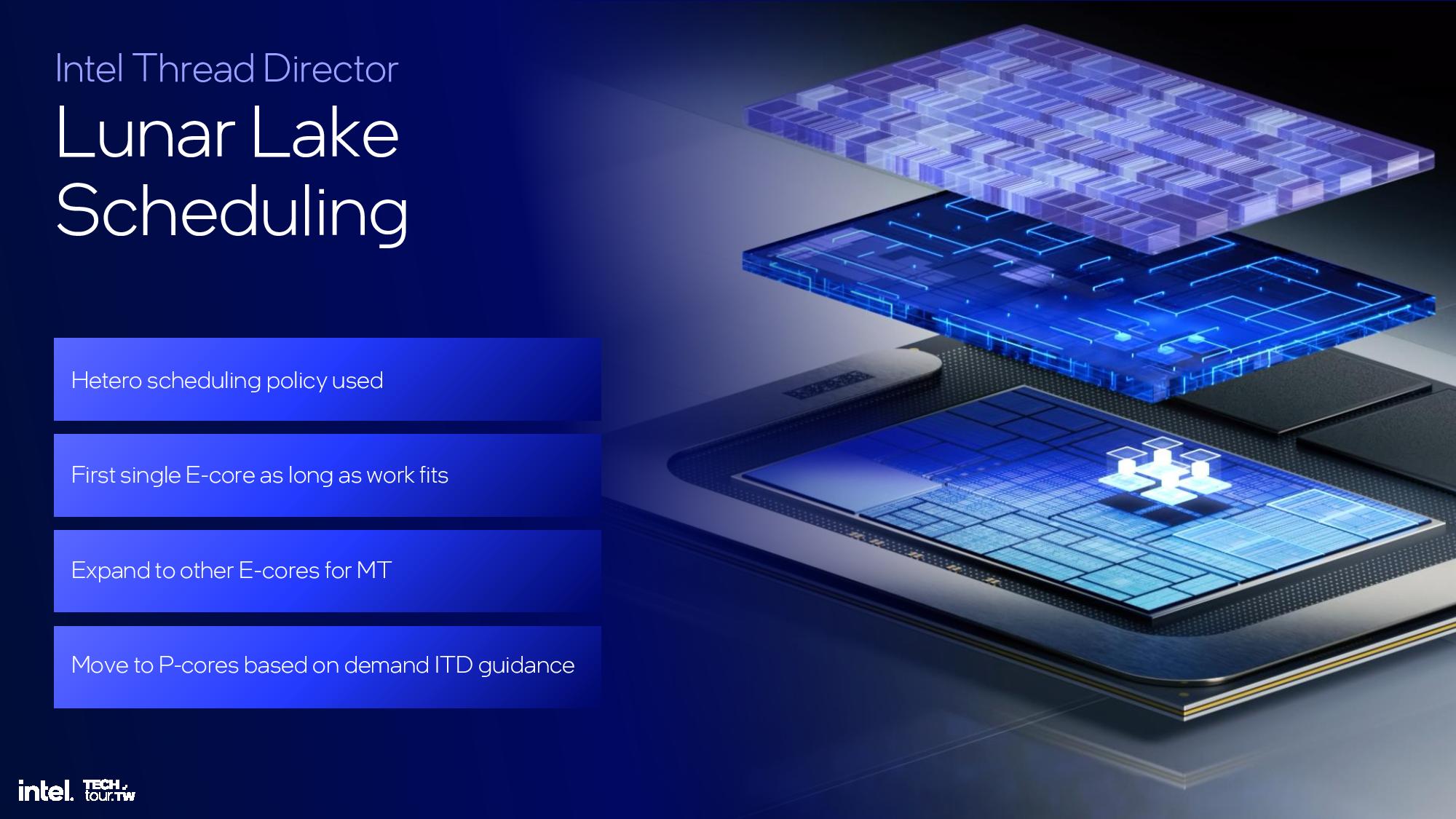
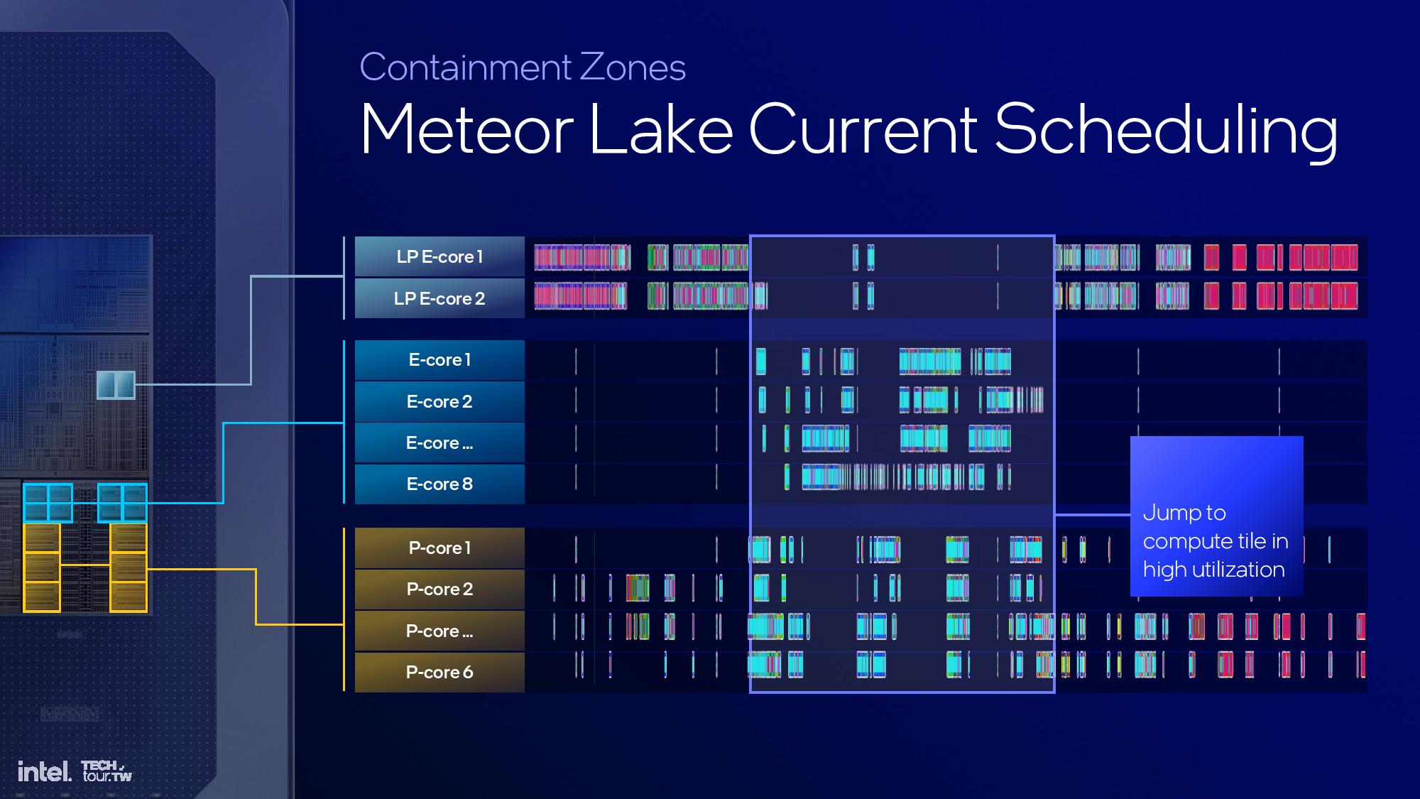
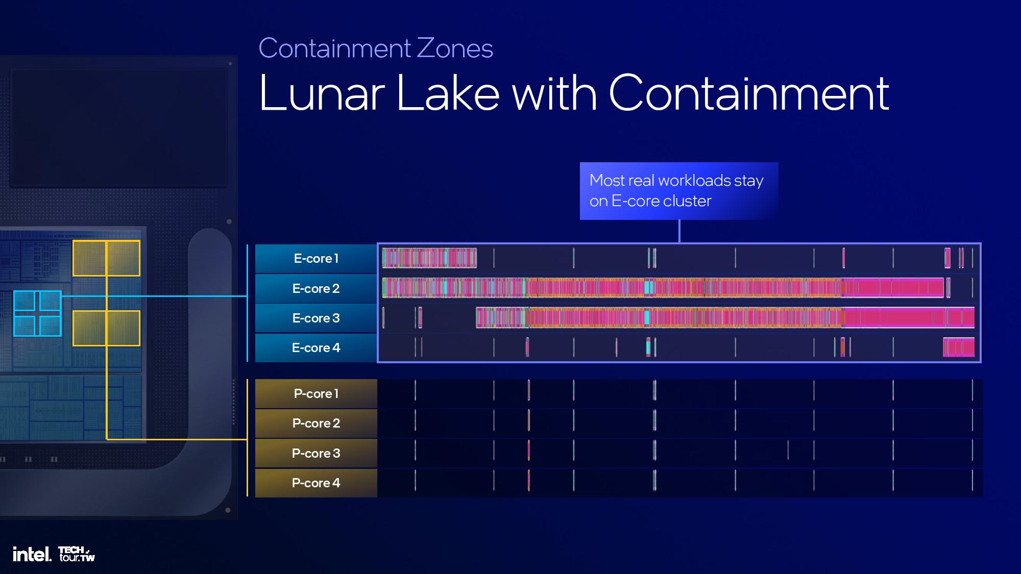

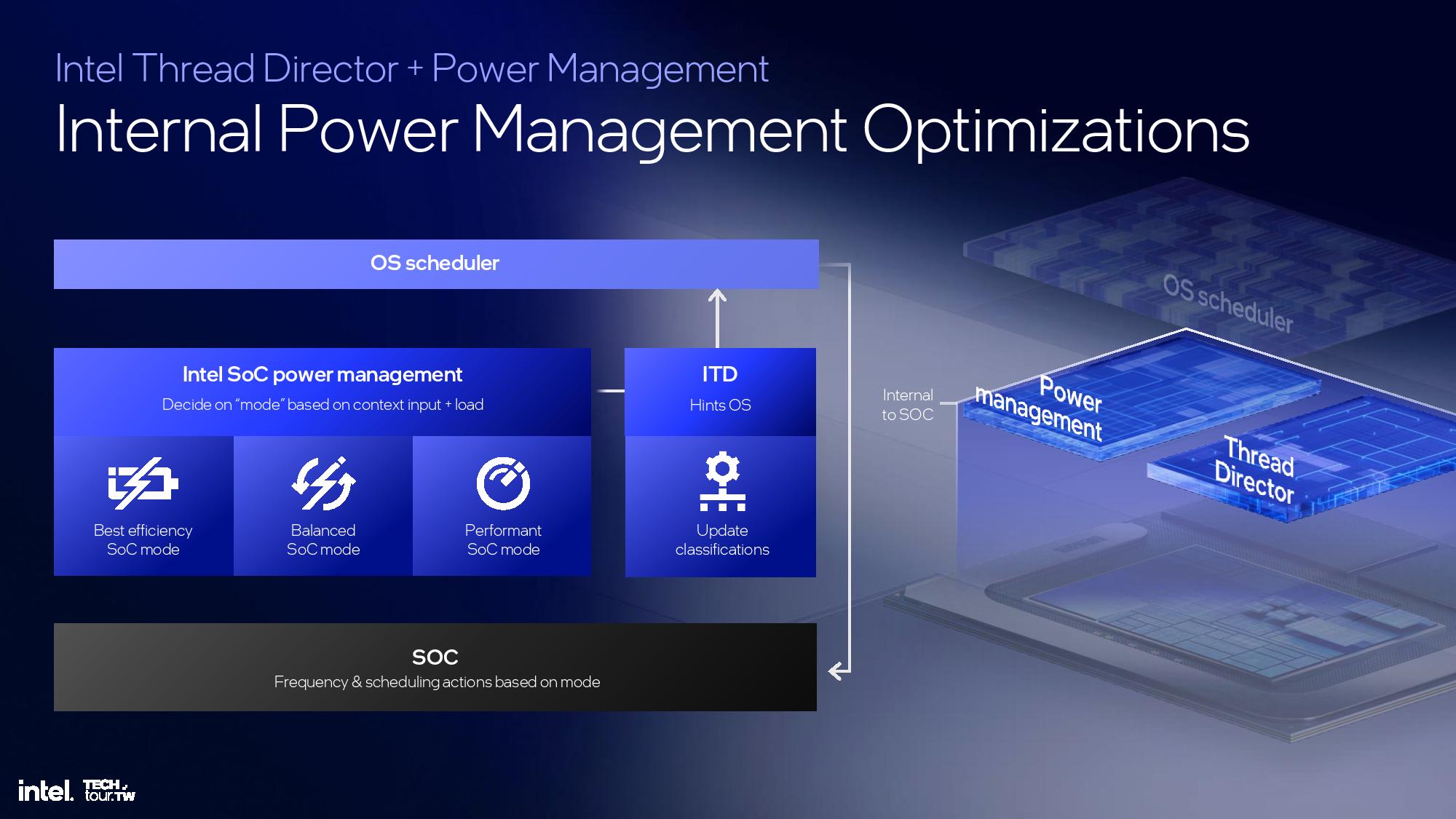
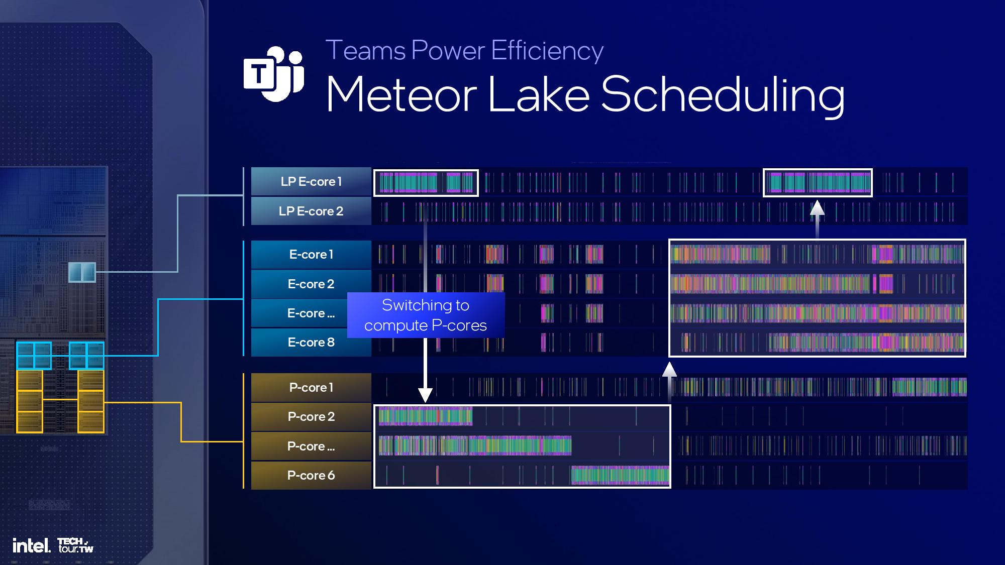
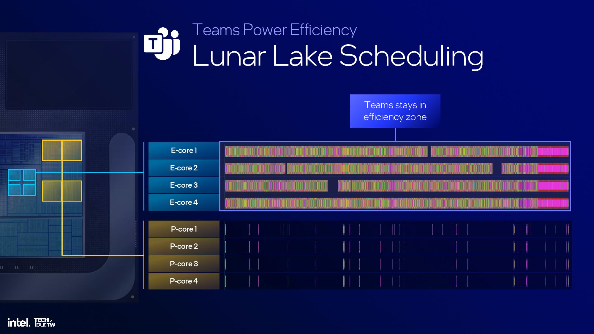
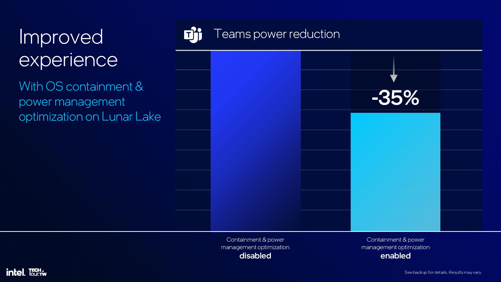
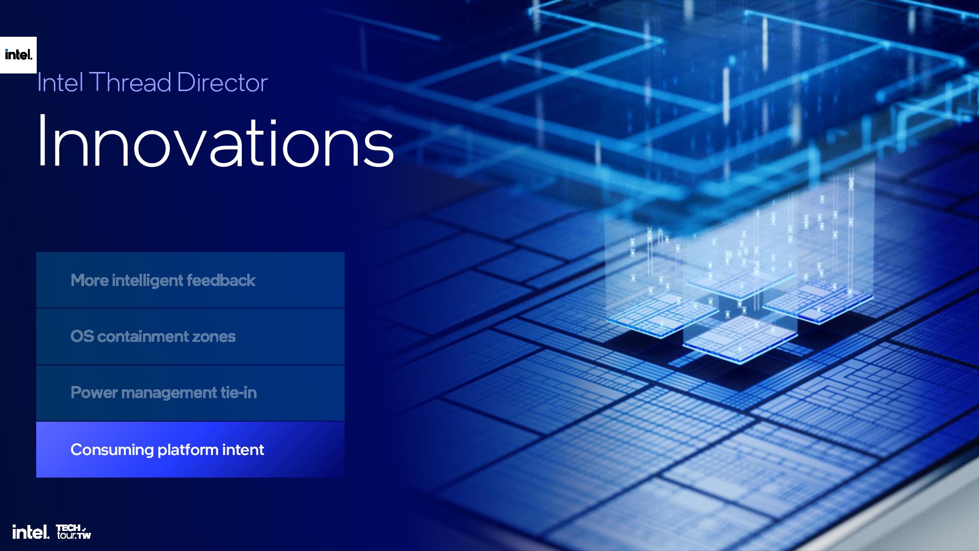
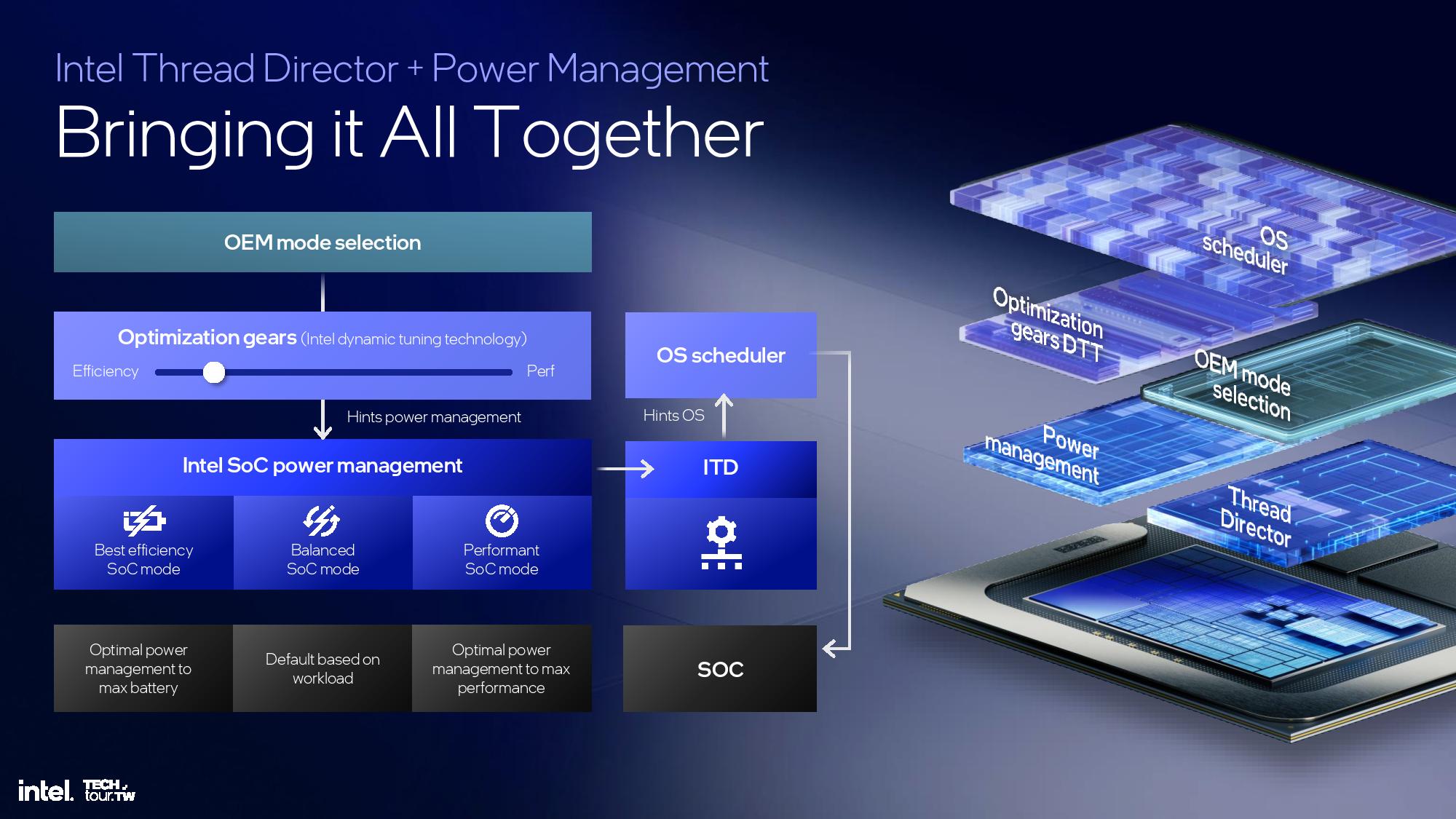
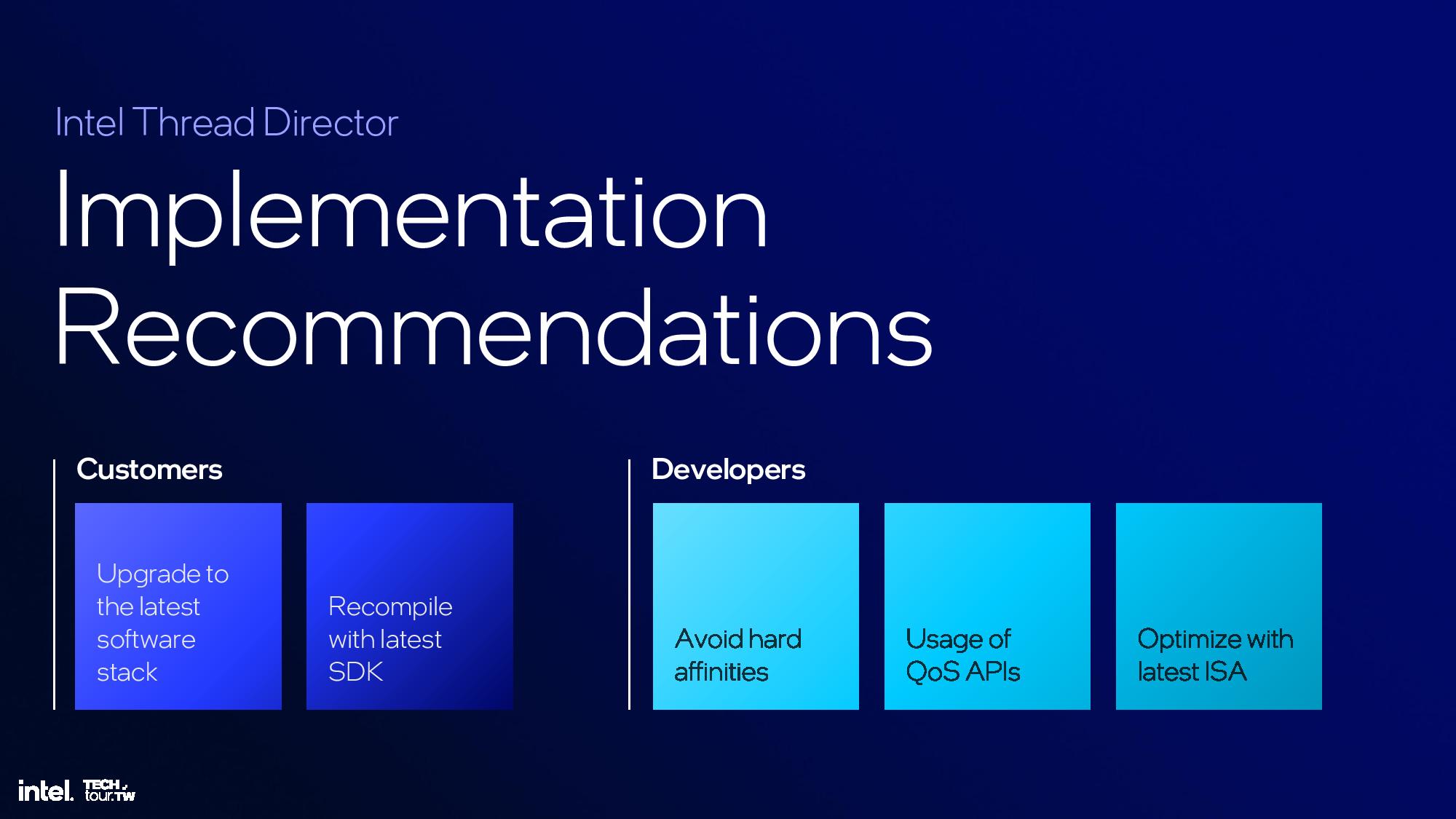
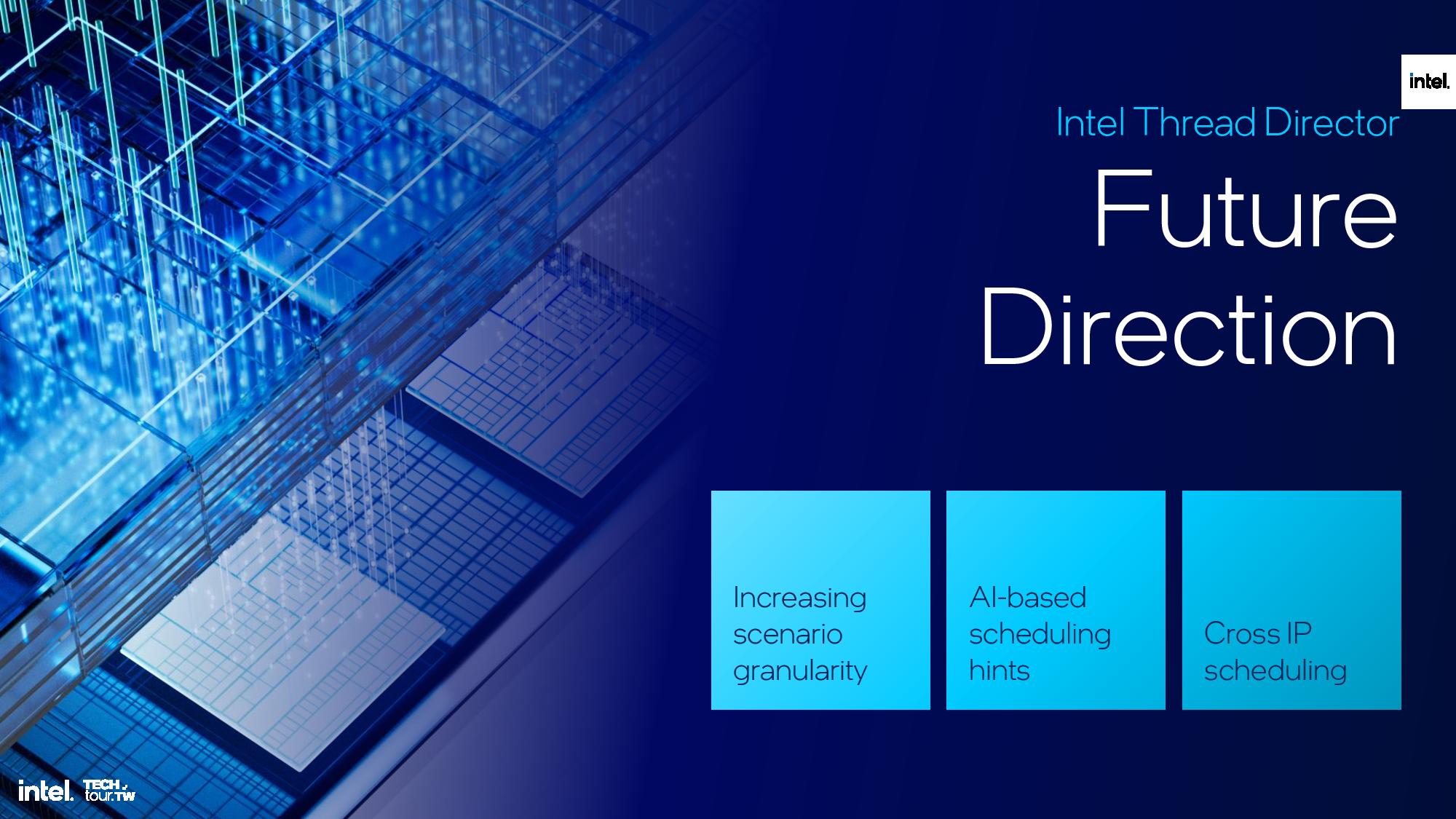
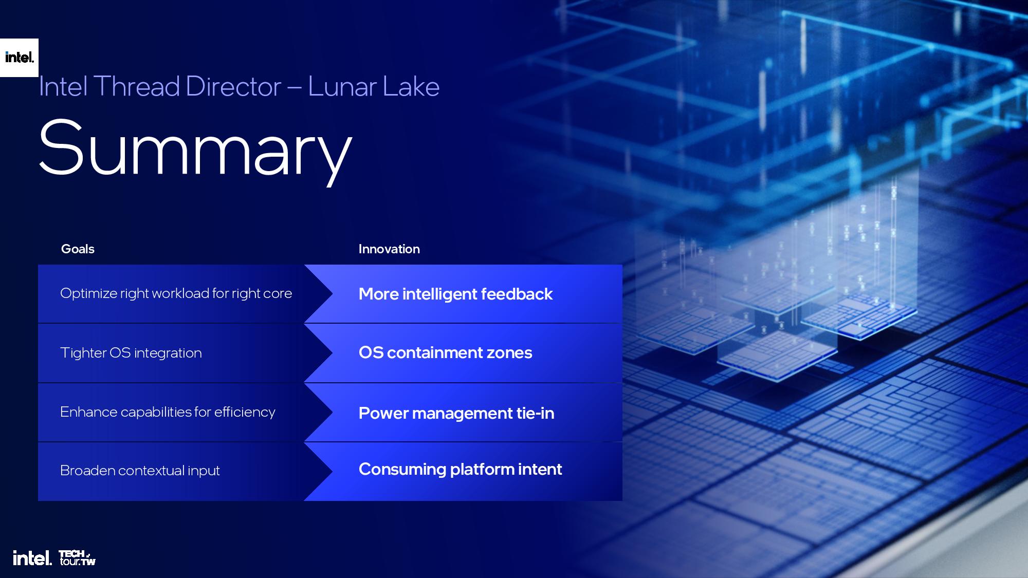
This is another area of the architecture that I wasn't able to attend the briefing, but we'll update this section once we have more time. The above slides provide most of the high-level overview.
Thoughts
Intel’s rethinking of its first-order priorities is important as it looks to fend off Apple’s M3, Qualcomm’s new Snapdragon X Elite, and AMD’s Ryzen AI 300 series processors. Intel will release Lunar Lake as two models, at least initially, but it hasn’t shared the final specifications for those models yet. Intel plans to ship 40 million AI-enabled processors by the end of the year, and Lunar Lake wafers are already in the company's fabs. The chips will arrive in shipping systems in Q3, 2024.
Intel’s Lunar Lake architecture, and all of the associated core IPs, represents a dramatic rethinking of the company’s design goals to a power-first design to maximize battery life and performance. The improved design methodology and CPU and GPU microarchitectures will soon filter down to Intel’s other mobile products, like the upcoming Panther Lake, its Arrow Lake chips for desktop PCs, and its data center Xeon 6 processors.
The current Meteor Lake processors were the first step on this road to placing multiple tiles on a single package, and Intel looks to make improvements in every aspect of the design with Lunar Lake. With more competition in the mobile sector, Intel needs its upcoming processors to be more revolutionary than evolutionary, and the architectural deep dive seems to indicate everything is in place. We'll find out this fall how it all comes together, and how Lunar Lake competes with other options.