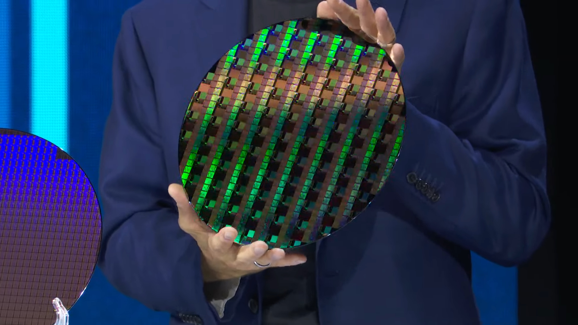
Intel this week revealed defect density metrics for its 18A (1.8nm-class) process technology and said that it was healthy at the Deutsche Bank's 2024 Technology Conference. The company also said that the number of customers potentially interested in using this production node was growing.
"I am happy to update the audience that that we are now, for this production process, we are now below 0.4 d0 defect density, this is now a healthy process," said Pat Gelsinger, chief executive of Intel, at the technology conference.
When it comes to defect density (D0), then it is commonly believed that a defect density below 0.5 defects per square centimeter is good (0.5 def/cm^2), so Intel 18A's 0.4 defects per cm^2 is a good result (at least on paper), especially considering the fact that the production technology is a few quarters away from entering mass production, at which point defect density will likely get lower.
It should be noted that this defect metrics can vary depending on process technology and applications. For example, defect density of TSMC's N7 and N5 process technologies was approximately 0.33 def/cm^2 three quarters before mass production, which is about the same point where Intel's 18A is today.
TSMC's N5 entered mass production with a 0.1 def/cm^2, according to a slide from the foundry published several years ago. N3's defect density was higher than N5's when it entered mass production, but it matched D0 of N5 in five or six quarters (i.e., the improvement curve of N3 matched that of N5 at the same time of their development, this does not mean that D0 of N3 and N5 are the same today).
Intel's own first products to use its 18A process technology will be the codenamed Panther Lake processor for client PCs and the Clearwater Forest processor for datacenters. Also, Intel's codenamed Diamond Rapids CPU is also set to use this node. Among external customers, Microsoft confirmed plans to use for a processor and the U.S. Department of Defense is set to use it for its chips. In total, Intel expects eight 18A tape-ins by mid-2025, including internal and external products.
Several weeks ago, Intel said it had released process development kit (PDK) 1.0 for its 18A node, which enables its own developers and customers to start or finalize their 18A chip designs.
"We now have a dozen of customers that are actively engaged with us around that 18A PDK," Gelsinger said. "We have eight product tape-ins that we expect to finish by the middle of next year."