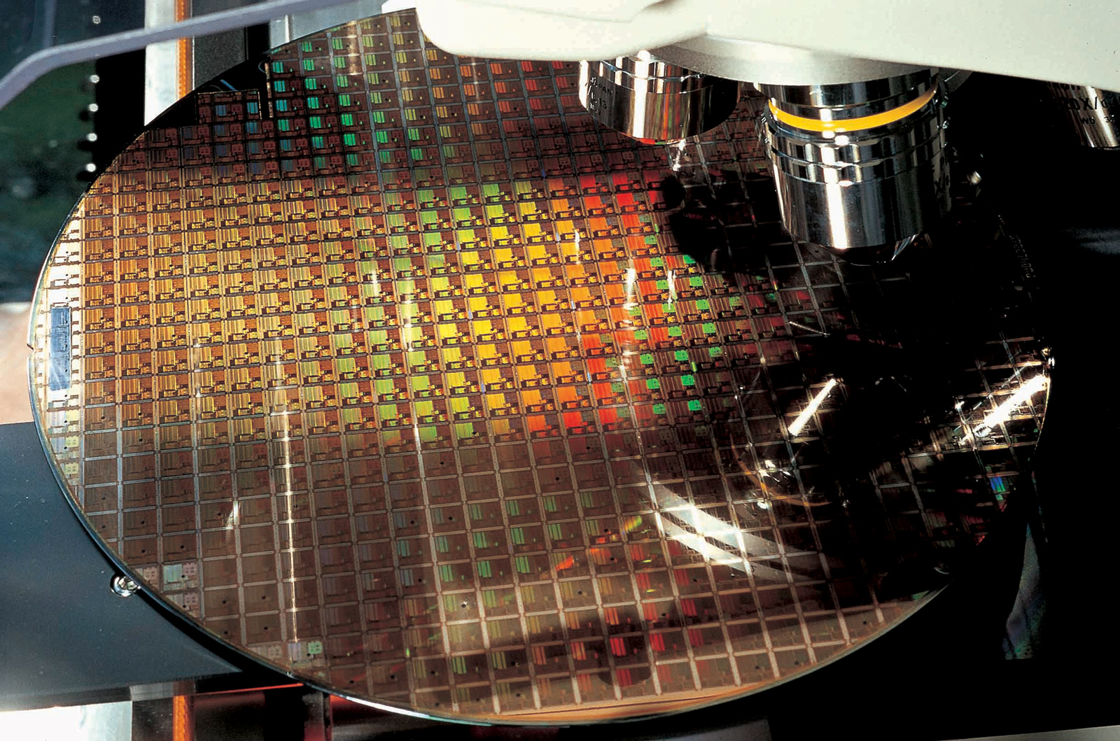
TechInsights and SemiWiki have published key details that Intel and TSMC disclosed about their upcoming 18A (1.8nm-class) and N2 (2nm-class) process technologies at the International Electronic Devices Meeting (IEDM). According to TechInsights, Intel's 18A could offer higher performance, whereas TSMC's N2 may provide higher transistor density.
Analysts at TechInsights believe that TSMC's N2 offers a high-density (HD) standard-cell transistor density of 313 MTr/mm^2, which far exceeds the HD cell density of Intel's 18A (238 MTr/mm^2) and Samsung's SF2/SF3P (231 MTr/mm^2). While the information more or less aligns with SRAM cell sizes for 18A, N2, and N3, as well as with TSMC's expectations for N2 and N3, there are some things to note.
First, this only concerns HD standard cells. Virtually all modern high-performance processors that rely on leading-edge nodes use a mix of high-density (HD), high-performance (HP), and low-power (LP) standard cells, not to mention capabilities like TSMC's FinFlex and NanoFlex.
Secondly, it is unclear how Intel's and TSMC's HP and LP standard cells compare. While it is logical to assume that N2 has a transistor density lead, it may not be as massive as the lead in HD standard cells. Third, in their papers presented at the IEDM event, both Intel and TSMC disclosed performance, power, and transistor density advantages of their next-generation 18A and N2 manufacturing processes over their predecessors. Still, there is currently no way to compare these two fabrication technologies head-to-head.
When it comes to performance, TechInsights believes that Intel's 18A will have a lead over TSMC's N2 and Samsung's SF2 (formerly known as SF3P). However, TechInsights uses a debatable method to compare the performance of the upcoming nodes, as it uses TSMC's N16FF and Samsung's 14nm process technologies as baselines and then adds announced node-to-node performance improvements from both companies to make its prediction. While this might serve as an estimate, it may not be entirely accurate.
On the other hand, Intel specializes in making high-performance processors, so 18A could be tailored for performance and power efficiency rather than HD transistor density. At the end of the day, 18A supports PowerVia, a backside power delivery network, and chips that use it might have performance and transistor density advantages over TSMC's N2, which does not support this capability. However, this does not mean that every 18A chip will use PowerVia.
When it comes to power, TechInsights analysts presume that an N2-based chip will consume less power than a similar SF2-based IC, as TSMC has typically led in power efficiency in recent years. As for Intel, this remains to be seen, but at least 18A will provide an advantage in this area.
There are a couple of other things to note. Intel's 18A is set to enter mass production in mid-2025 when Intel begins production of its Core Ultra 3-series ‘Panther Lake' processors, which will be available later this year. By contrast, TSMC's N2 is slated for high-volume manufacturing in late 2025, and the first products produced on this node will not be available until mid-2026 at the earliest, with mass-market products expected in Fall 2026. Samsung does not disclose when exactly its SF2 enters HVM, only stating '2025,' which could mean any time from Q1 to Q4 this year.