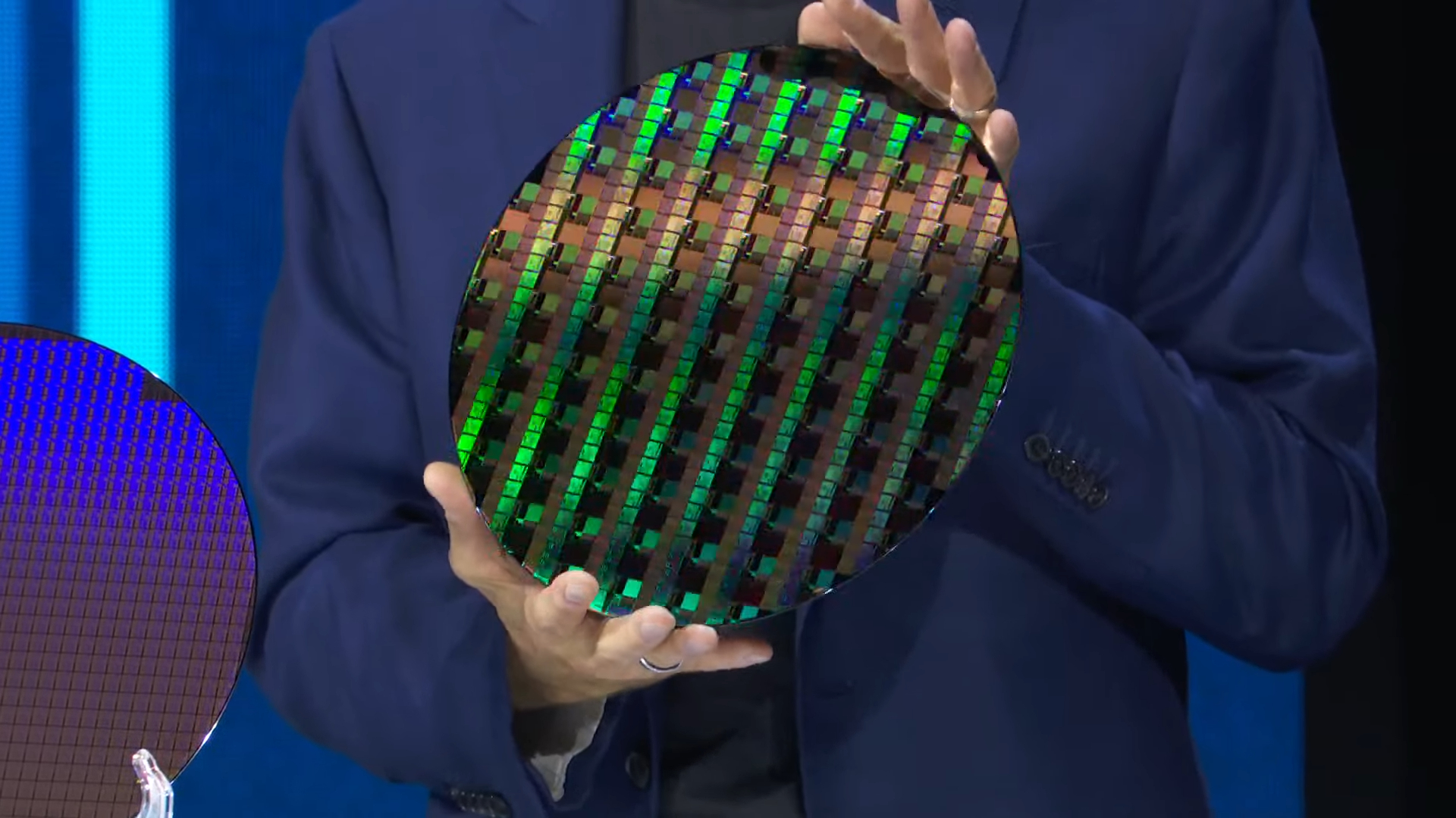
While the whole market was looking at the appointment of Lip-Bu Tan as Intel chief executive, there was another major development at the company this week: The first 18A (1.8nm-class) wafers are running around Intel's Arizona fab. Intel's Fab 52 and Fab 62 in Arizona are high-volume production facilities, so running 18A fabs there is a major milestone for the company.
The most important $INTC announcement today wasn't the CEO announcement.It was 18A wafers coming off the line at their new fab in Arizona. This fab is only meant to start output mid 25 so it looks like it is ahead of schedule.Congratulations to all the @Intel engineers! 🔥🔥 pic.twitter.com/730Otd4B3pMarch 13, 2025
"Exciting Milestone for Intel 18A," wrote Pankaj Marria, an engineering manager at Intel, in a LinkedIn post that was eventually hidden but captured by @Mojo_flyin on X. "Proud to be part of the Eagle Team, leading the way in bringing Intel 18A technology to life! Our team was at the forefront of running the initial lots right here in Arizona, marking a key step in advancing cutting-edge semiconductor manufacturing."
Up until recently, Intel processed wafers on its 18A production technology at its site near Hillsboro, Oregon, where new manufacturing processes are developed. While the company can volume produce chips in Oregon as well, porting this new fabrication process to a brand-new fab in Arizona is indeed a milestone for the company.
For now, the company is running test wafers to ensure that the fabrication process transfer is a success, but eventually the fab will start running actual chips for commercial products.
Intel is set to mass produce compute chiplets for its upcoming codenamed Panther Lake processors on 18A technology later this year. Eventually, Intel's 18A production node will be used to make Intel's Xeon 7 codenamed Clearwater Forest processor for datacenters.
Intel pins a lot of hope on the upcoming 18A fabrication process. The manufacturing technology relies on gate-all-around RibbonFET transistors that promise to increase performance and cut down power consumption.
It also features backside power delivery, which is meant to ensure steady power delivery to power-hungry processors and increase transistor density by decoupling signal and power wires within a chip.
"This achievement is a testament to the hard work, innovation, and dedication of everyone involved. The Eagle has landed, and this is just the beginning! Developed and Made in America the world's smallest node," Marria added.