Intel on Monday detailed its implementation of a backside power delivery network (BS PDN) that will be a part of its Intel 18A and 20A (18/20 angstroms, 1.8/2.0nm-class) fabrication processes. In addition, the company also revealed more information about the benefits this technology provided for its internal Intel 4 + PowerVia node designed specifically to best BS PDN.
Backside Power Delivery
Intel's 18A and 20A manufacturing technologies will introduce two key innovations: RibbonFET gate-all-around field-effect transistors (GAAFETs) and PowerVia backside power delivery network. The advantages of GAA transistors have been discussed previously and are beyond the scope of today's announcement. We'll focus instead on backside power delivery.
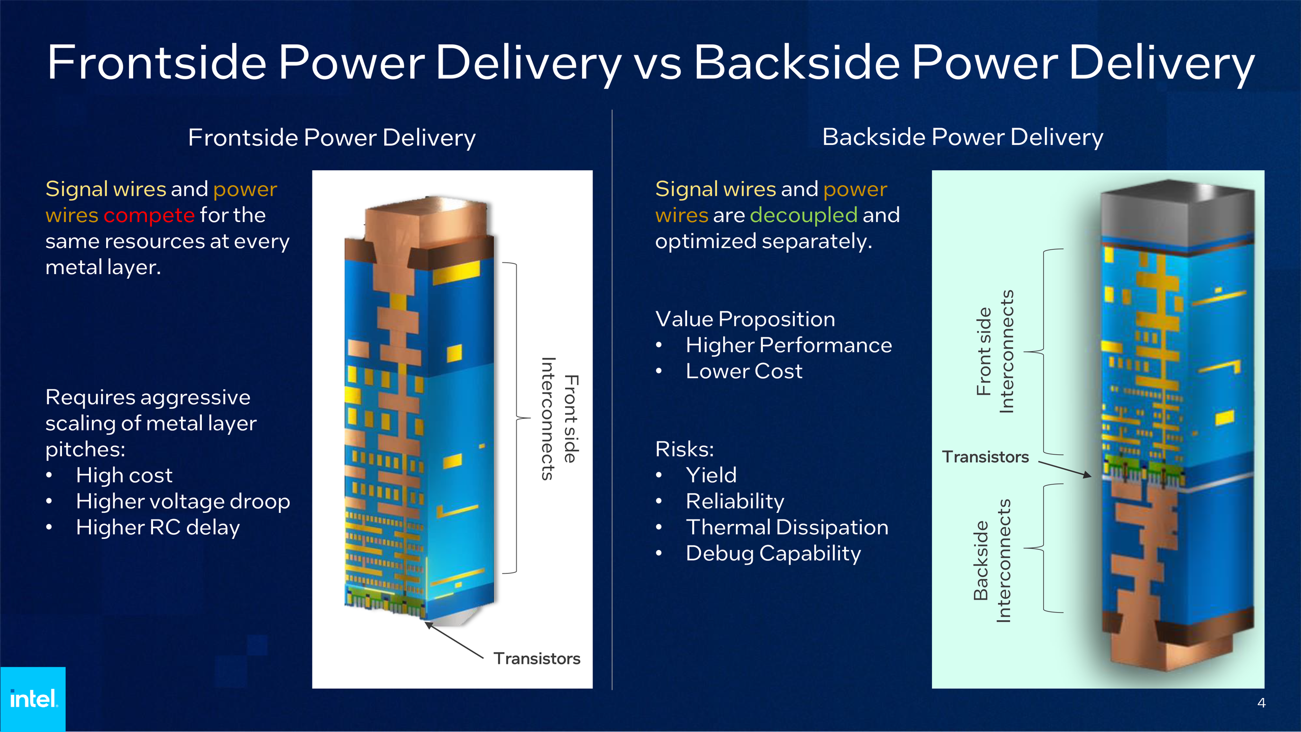
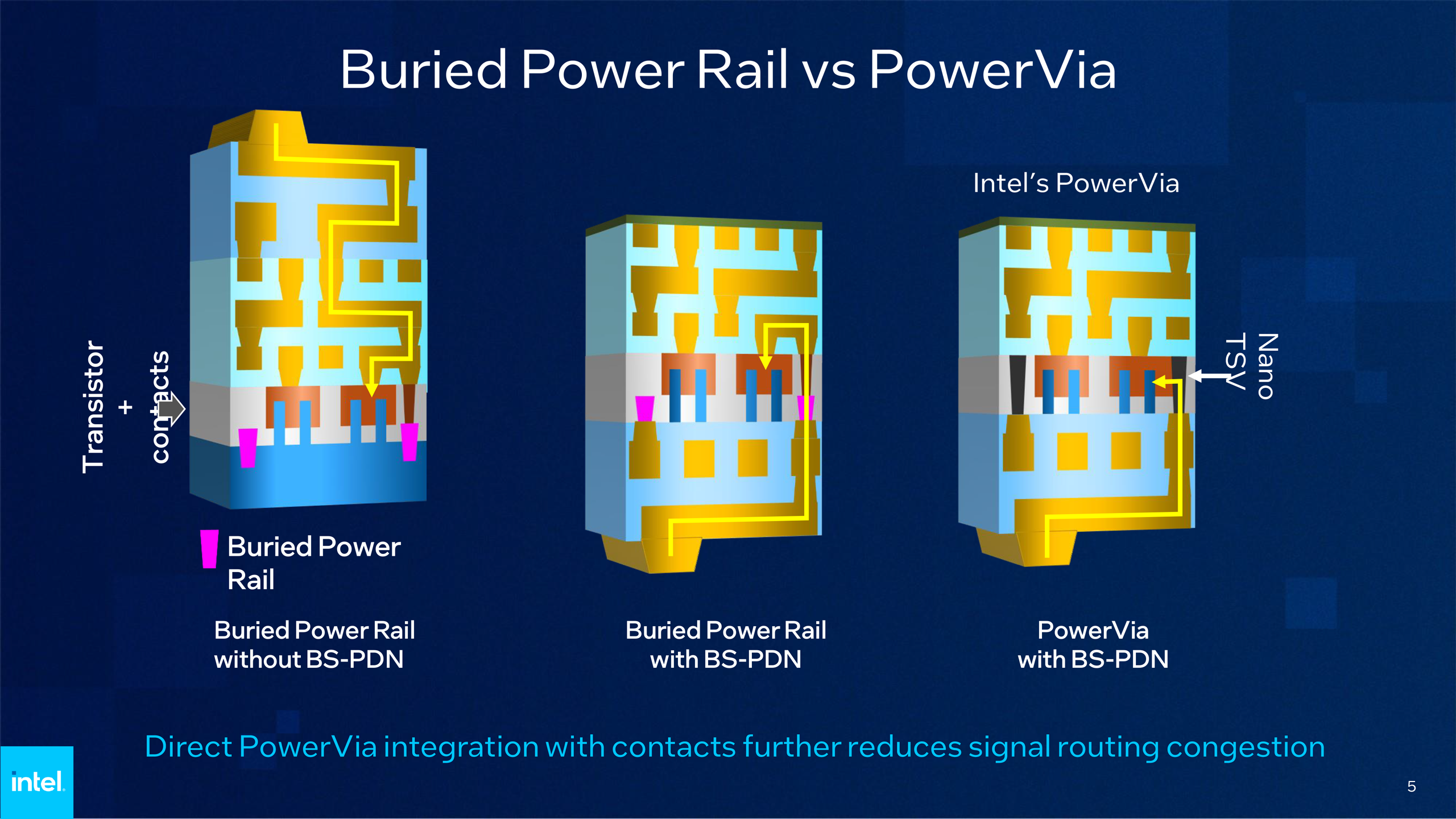
The backside power rail aims to separate power and I/O wiring, shifting power lines to the back of the wafer. This method tackles problems such as increased via resistances in the back-end-of-line (BEOL), ultimately improving the performance of transistors and lowering their power consumption. It also eliminates any possible interference between the data and power wires and increases logic transistor density.
Over time, BD PDN will become a standard chip feature, but for now Intel considers it a major breakthrough innovation akin to strained silicon at 90nm in 2003, Hafnium-based high-K metal gate at 45nm in 2007, and FinFET at 22nm in 2012.
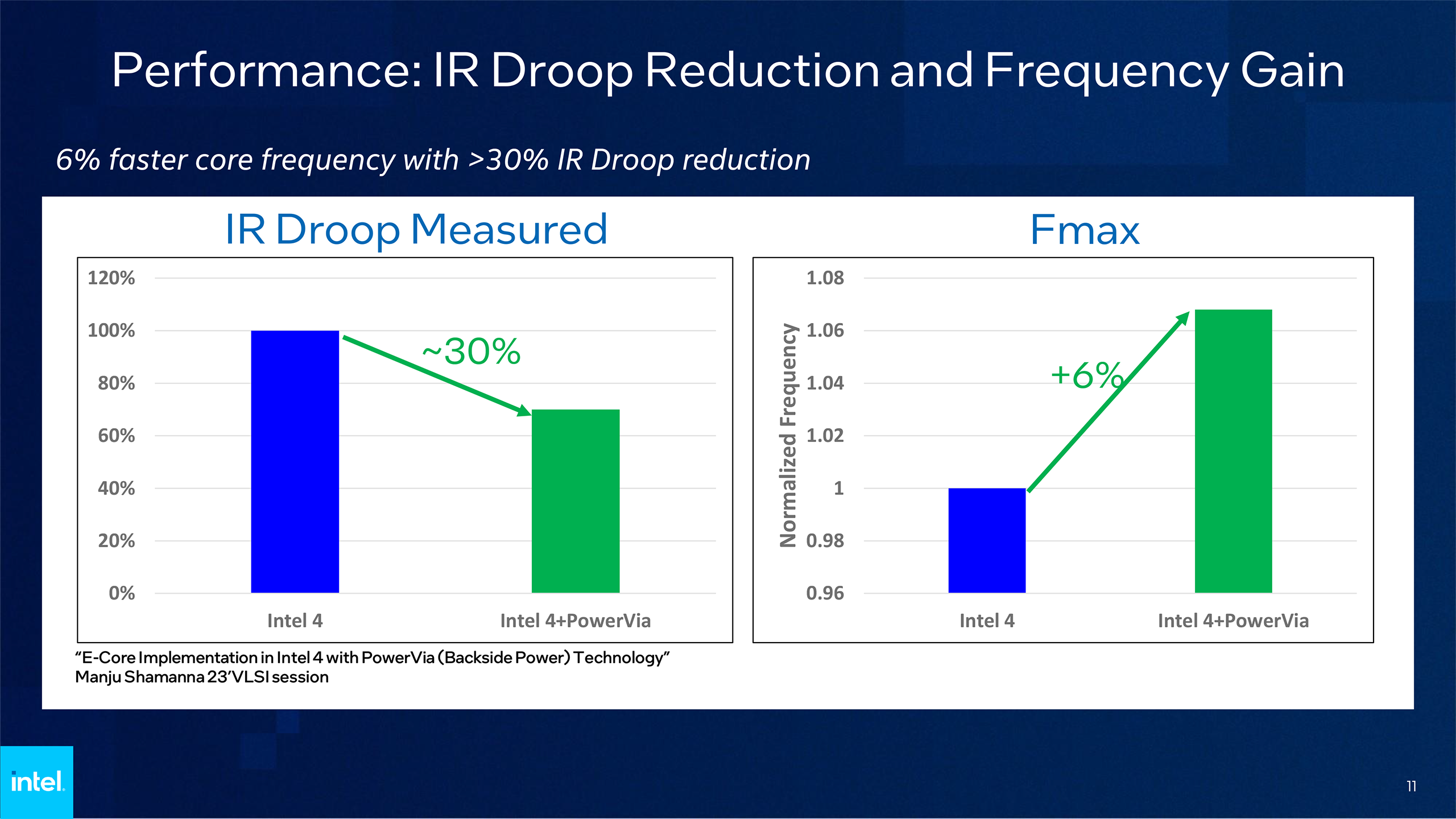
Intel says that when implemented in a test chip on an internal process node, its backside PDN enabled it to increase clock speed by over 6%, reduced IR voltage droop by 30%, and increased cell utilization over large areas of its E-core die to over 90%. Despite the benefits, implementing and building a backside power delivery is a challenge for several reasons.
Building PowerVia Backside PDN
Building a backside PDN is very different from traditional frontside power delivery. Production of even the most advanced chips is pretty straightforward these days. Fabrication of every wafer starts from the most complex M0 transistor layer with pitches as small as 30nm (for Intel 4 node) using the most sophisticated manufacturing tools like EUV scanners. Then chipmakers build less complex transistor layers on top of the first one, gradually increasing sizes as they need to connect all the layers and power all the transistors.
The actual physical wires for I/O and power look gigantic when compared to the transistor layers, and it gets harder and costlier to route them properly with every new generation.
Processing a wafer with chips featuring Intel's PowerVia BS PDN involves producing all the complex logic layers as well as signal wires, then flipping the wafer and building the power delivery network 'on top' of the logic. On paper, such a 'flip' does not look like a big deal. However, it adds quite a number of process steps, including removal of 'excess' silicon from the wafer to build the PDN on top of the logic transistors, CMP clean, metrology, lithography, and etching, to name a few.
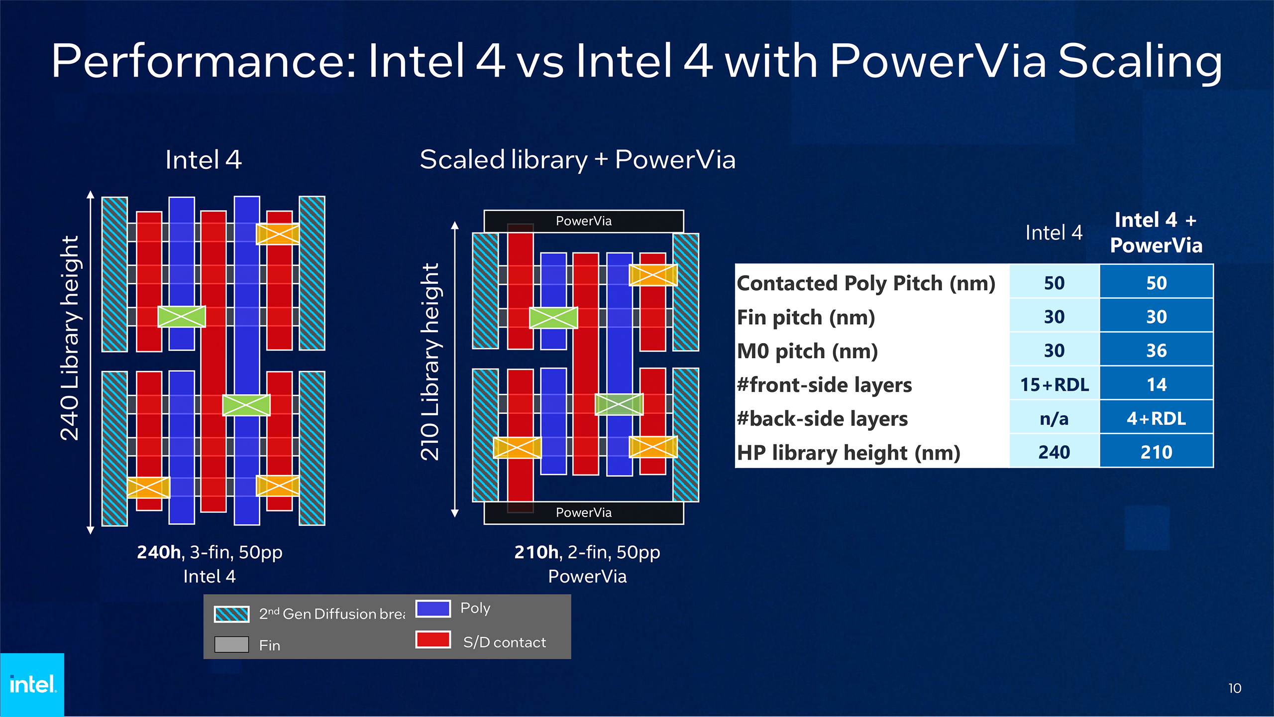
Such a process loop may not require the most advanced tools in the fab, but it still costs money. Indeed, an Intel slide indicates that the Intel 4 process technology uses 15 metallic layers and a redistribution layer (RDL), whereas Intel 4 + PowerVia uses 14 front side layers, four back side layers, and an RDL, which increases total number of layers to 18 + RDL.
"Transistors are built first, as before, with the interconnect layers added next," said Ben Sell, vice president of Technology Development at Intel. "Now the fun part: flip over the wafer and polish everything off to expose the bottom layer to which the wires […] for power will be connected. We call it silicon technology, but the amount of silicon that's left on these wafers is really tiny."
There are several factors to consider with a backside PDN. First up, it changes the manufacturing process drastically, so Intel had to find a way to ensure high yields despite radical changes. Second, Intel had to ensure that the backside PDN is as reliable as its current PDN and performs as intended. Third, as I/O and power wires are now located on both sides of transistors, it will get more challenging to cool down chips going forward. Fourth, it gets significantly harder to debug chips as now Intel has to remove backside power interconnects to access transistor layers.
There is another peculiarity about Intel's PowerVia process too. Because Intel removes excessive silicon from the back of the wafer, it believes it loses rigidity, which is why it bonds a carrier wafer on the signal side of the wafer to hold the construction together. That carrier wafer also gets thinned down eventually, but its addition is also a complicated (and probably necessary) process step.
Another thing about Intel's PowerVia backside PDN is that it doesn't use buried power rails with BS PDN, but instead will rely on nanoscale through silicon vias (TSVs) to deliver power right to the transistor layer. This is obviously why the company calls its technology PowerVia.
Testing Backside Power Delivery Network
Now that Intel is no longer the indisputable leader of the chip market with the best process technologies, the company could not risk a potential point of failure in one of its next generation nodes. So, it decoupled development of RibbonFET GAA transistors and PowerVia BS PDN to make the development process a little bit easier by working on RibbonFETs with a regular PDN and then debugging PowerVia with proven FinFETs.
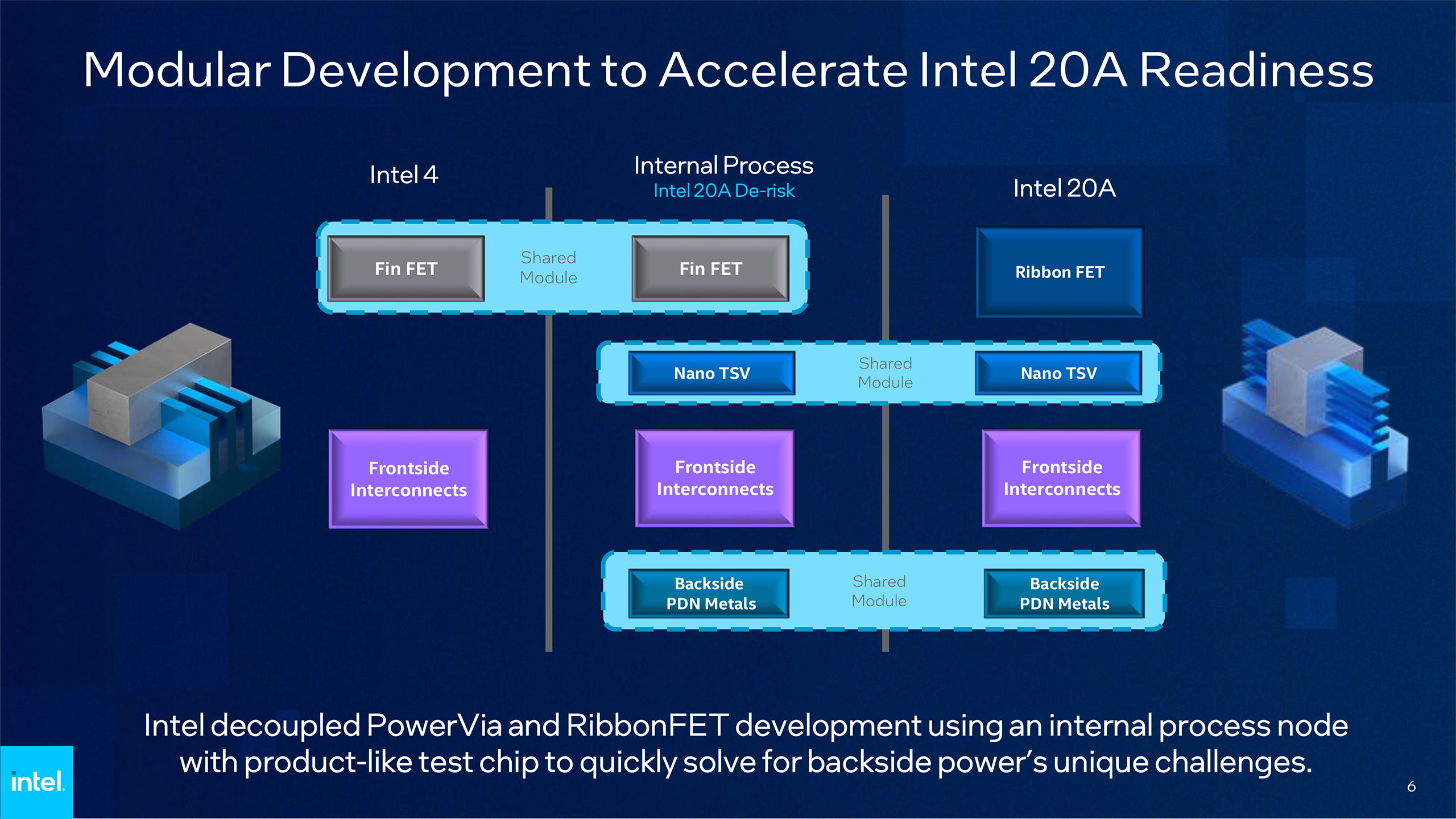
To test its PowerVia backside power delivery network, Intel built a special manufacturing process based on its Intel 4 node that uses proven FinFET transistors, but it comes with a backside power rail instead of a traditional power rail. This process is naturally called Intel 4 + PowerVia and it is used for one test chip codenamed Blue Sky Creek.
Intel's Blue Sky Creek test chip uses two dies, each featuring four energy-efficient cores based on the Crestmont microarchitecture. These are designed to operate at 3 GHz at 1.1 Volts. The test vehicle was designed for two purposes only: explore the advantages of the PowerVia BS PDN and remove risk from the future 20A/18A process technologies by testing all of the things associated with the novel power delivery network, including yields, reliability of PDN and the chip, cooling, and debugging.
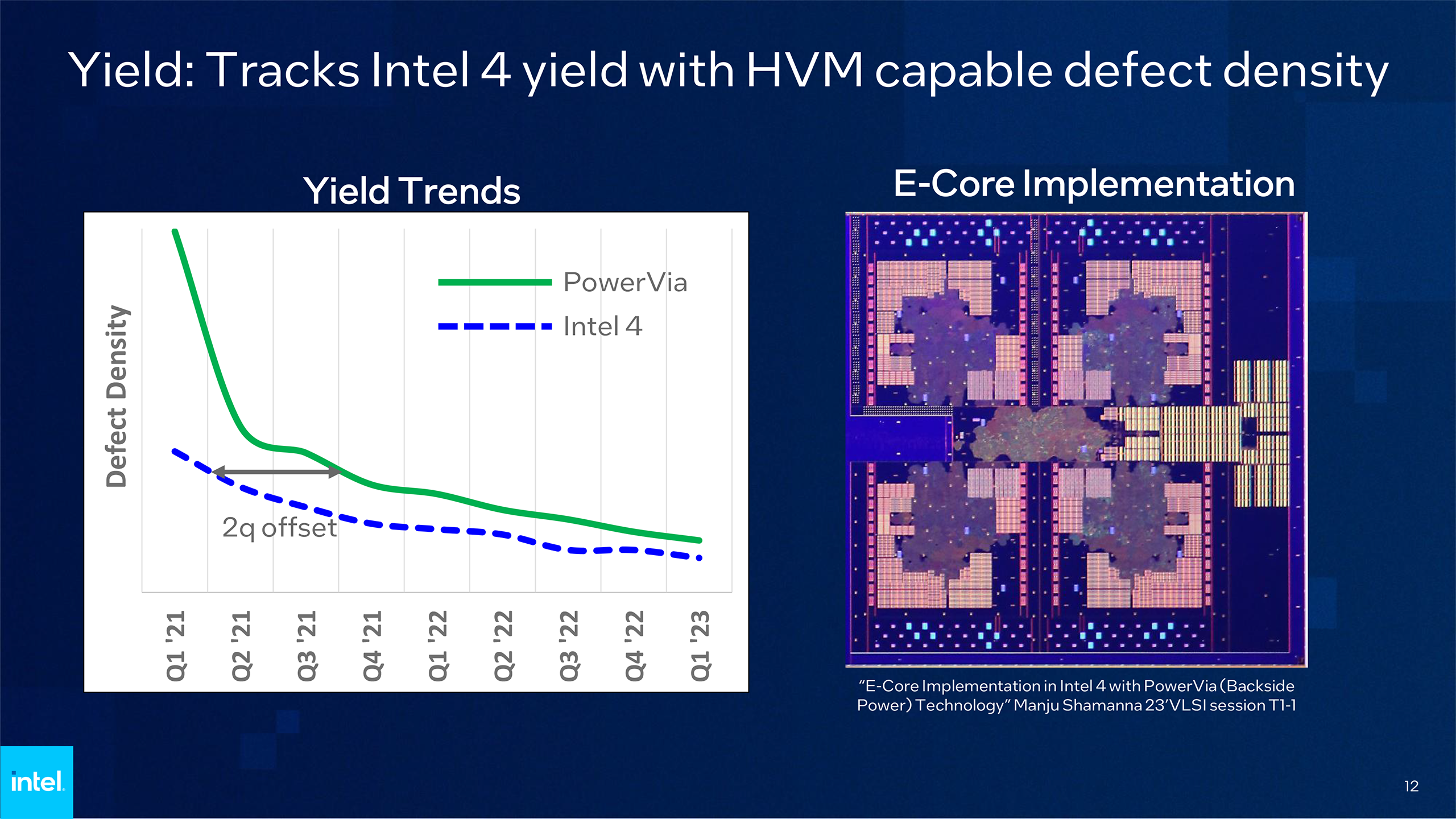
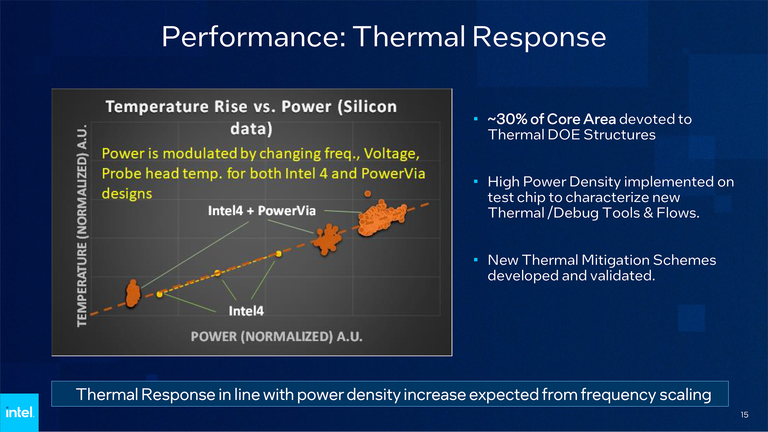
When it comes to yields, Intel says that the defect density of the test chip implemented on Intel 4 and on Intel 4 + PowerVia are nearly the same. Reliability and transistor characteristics goals also met expectations required for production. Furthermore, thermals of the test vehicle were in line with expectations. Meanwhile, Intel admits that cooling will be a challenge with backside PDN, so it has developed new thermal mitigation schemes to cool down next-gen chips.
"Normally you use the silicon side also for heat dissipation," explained Sell. "So, now you have sandwiched your transistors and the question is, 'Do we have a thermal problem? Do we get a lot of local heating?' At this point you can probably guess the answer: no."
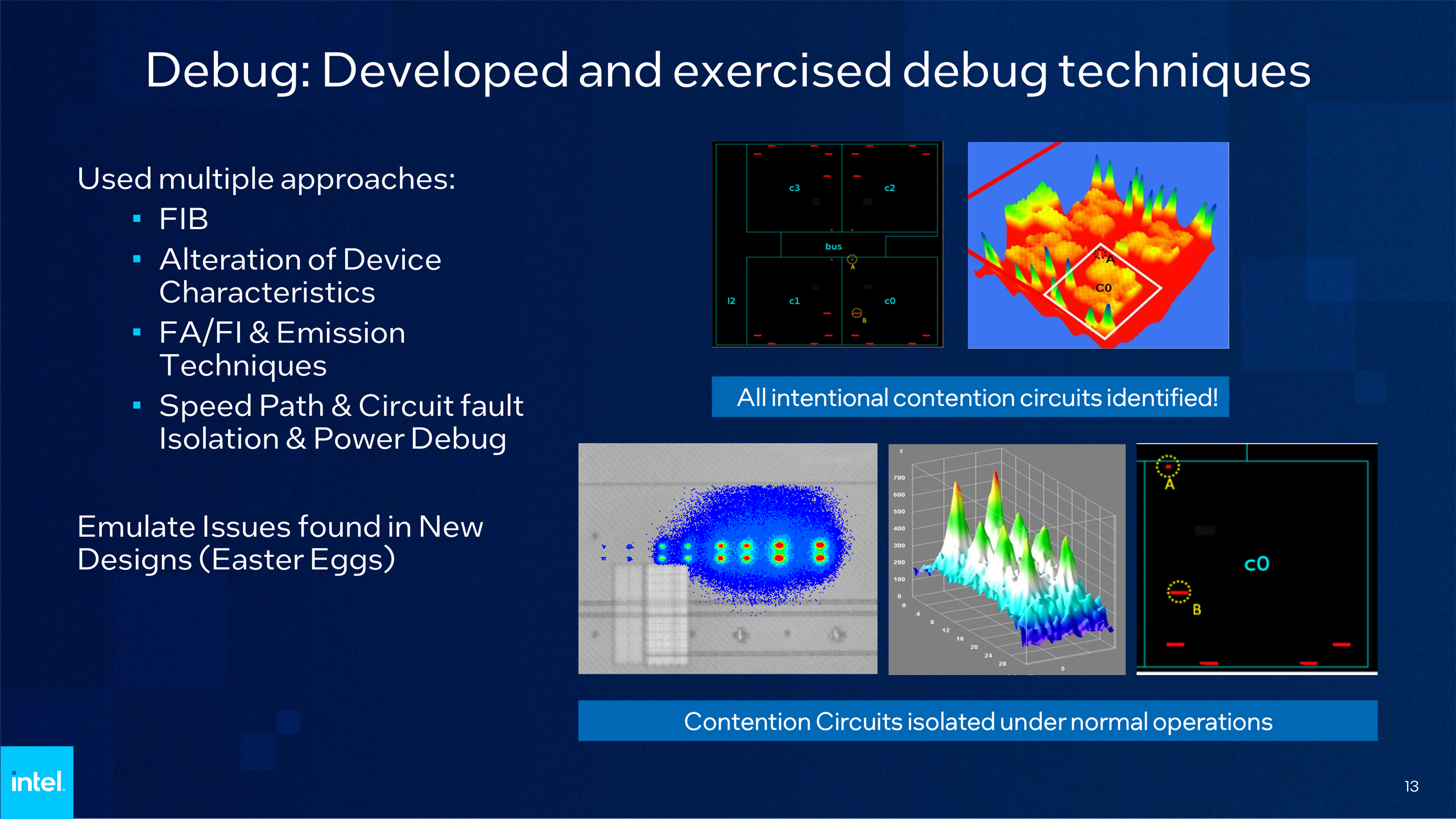
Debugging was arguably one of the most complicated parts, but luckily Intel's validation engineers have found a way to overcome the difficulties.
"There were a lot of concerns and hesitancy and that was probably the hardest thing to figure out — how to do debug on this new backside power delivery," said Sell. "To make things even more challenging, the test chip design team intentionally added some 'easter egg' errors to the chip, unbeknownst to the validation team. The good news? They found the bugs. We have made tremendous progress over the last couple of years in developing those debug capabilities and proving them on Blue Sky Creek."
Intel's PowerVia BS PDN Coming in 2024
Intel's first publicly available process technologies to use its PowerVia backside power delivery network will be its 20A and 18A nodes that will be production ready in 2H 2023 and 1H 2024, respectively. Intel's first client CPU to be made on the 20A fabrication process is Arrow Lake, which is expected to launch near mid-2024 or earlier.
Intel's 18A and 20A manufacturing technologies are developed both for the company's own products and for customers of Intel Foundry Services, so PowerVia promises to be a benefit both for Intel and its IFS clients. Whether or not PowerVia BS PDN will be a tangible benefit is something only time will tell, but it is noteworthy that Intel is the first company that is ready to make chips with backside power delivery, as TSMC is only expected to offer a similar technology in late 2026 to early 2027.


