Having joined Intel at a tough time and doing his best to revive the company before retiring, Pat Gelsinger is yet to see the fruits of his decisions as the chief executive of Intel. However, based on his claims, the 18A process technology — the pinnacle of his five nodes in four years plan — is a success. Being ousted by the board, Gelsinger now has more time to respond to messages on X, which adds some color to what's happening with Intel's node development.
Pat Gelsinger responded to Patrick Moorhead's post claiming that a rebuffed story about Broadcom being disappointed with Intel's 18A due to low yield was 'fake news.' The original story emerged in early September, right after Intel's then-CEO Pat Gelsinger disclosed the defect density (D0) of 18A, which back then was 0.4 def/cm^2.
"I am so very proud of the TD/18A team for the incredible work and progress they are making," Gelsinger wrote in an X post.
Given that 18A was several quarters away from mass production at that time, such a defect density was good enough, though worse than that of TSMC. For instance, the defect density of TSMC's N7 and N5 fabrication processes was about 0.33 def/cm2 three quarters before mass production, which was the same point where Intel's 18A was in early September.
It is commonly believed that a defect density below 0.5 defects per square centimeter is good (0.5 def/cm^2), though when it comes to the yield of actual chips, everything depends on the size of the die.
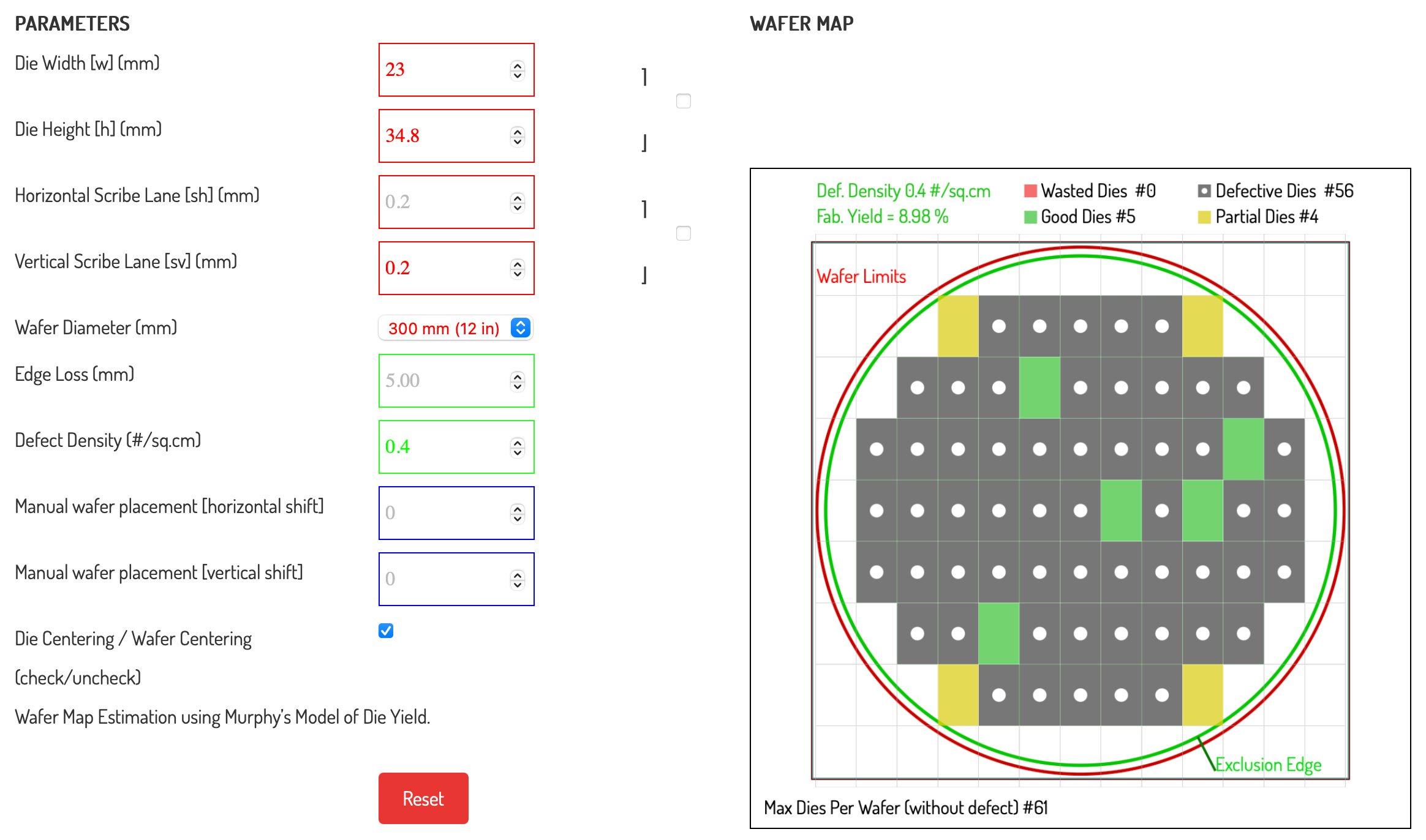
Broadcom is known for its gigantic system-in-packages for AI with compute chiplets close to the size of a reticle, which in the case of EUV lithography tools is 858 mm^2. Let's assume we are dealing with 800 mm^2 dies, which is the size of one Nvidia's Blackwell GPU chiplet (there are two chiplets per B100/B200 processor). In this example, there are 59 - 65 die candidates on a 300-mm wafer (assuming that we are dealing with a hypothetical 23 ´ 34.8 mm die), depending on various parameters. With a defect density of 0.4 def/cm^2, that gives us five perfect dies per wafer at a yield of around 9%. In the case of a defect density of 0.2 def/cm^2, we are already talking about 15 perfect dies and a yield of 24.9%.
There are several catches to be aware of in such a calculation. First, both Broadcom and Nvidia implement huge redundancies in their designs, so even with a relatively high defect density, they can get enough sellable die to justify the production of a 300-mm wafer using an advanced node. Depending on the client and contract, this might be at $20,000 per wafer, which means that their actual yield is well above the one we got from a publicly available yield calculator.
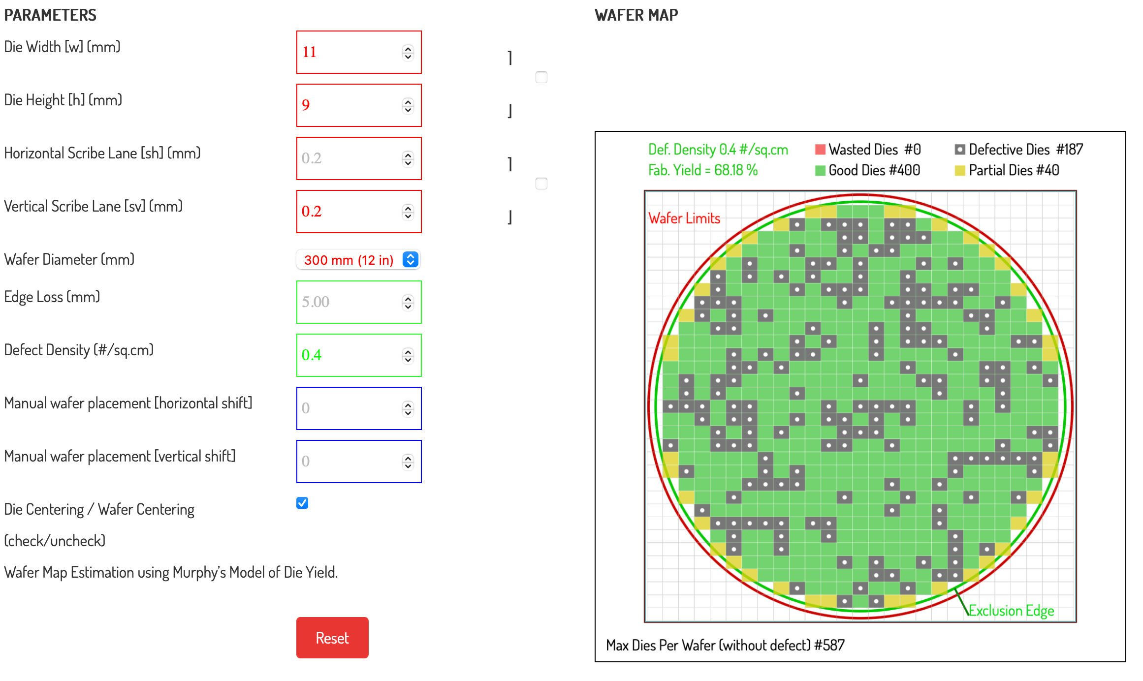
Secondly, not all processors are large. For example, Apple's A18 Pro system-on-chip for iPhone 16 Pro smartphones is 105 mm^2, and this is a very big processor for consumer devices. 105 mm^2 (let's assume it is an 11´9 mm design) gives us 625 die candidates per 300-mm wafer, and at a defect density of 0.4 def/cm^2, it gives us 587 perfectly yielded dies at a 68.2% yield. Again, Apple probably implements loads of redundancies into its designs, so the actual yield of sellable chips is higher.


In general, Intel says its 18A process technology shows promising defect density figures of 0.4 defects per square centimeter for now. While this density is slightly higher than TSMC's benchmarks at comparable stages of development, it is within industry standards for advanced nodes and sufficient for generating usable yields depending on die size and design redundancies. Larger dies, like Broadcom's and Nvidia's AI chiplets, face more significant yield challenges, but advanced redundancy techniques should probably mitigate these issues, enabling a viable number of sellable chips. Meanwhile, smaller processors, such as Apple's A18 Pro, achieve significantly higher yields even at the same defect density.


