China's Yangtze Memory Technology Corp is readying its next-generation 3D NAND memory architecture — Xtacking 4.0 — despite severe sanctions against the company, according to a document seen by Tom's Hardware. The company has no plans to increase the number of layers with the two Xtacking 4.0 devices currently in development, but the family may get broader over time.
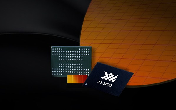
YMTC's Xtacking 4.0 lineup that the company has disclosed to some industry peers so far includes 128-layer X4-9060 3D TLC and 232-layer X4-9070 3D TLC NAND devices, which could eventually be used to build some of the best SSDs. The company plans to use string stacking for both. So technically, it will produce 3D NAND arrays with 64 and 116 active layers, which enables wafer fab equipment makers to keep supplying it with necessary tools without directly breaking U.S. export rules (so long as they obtain an export license from the U.S. Department of Commerce).
It is unclear precisely what advantages YMTC's Xtacking 4.0 memory will bring, but typically Yangtze Memory has increased data transfer rates and storage density with every new node. Given that the company faces severe restrictions and cannot obtain all the tools it needs, Xtacking 4.0 could somehow address its limitations. Plausible advances would include increasing the number of planes to boost parallelism and bitline/wordline optimizations to improve latency. As with any semiconductor, a tighter-tuned variant could also offer improved yields.
YMTC has been producing its 232-layer 3D TLC NAND memory featuring its Xtacking 3.0 architecture in high volumes for over a year now and more recently expanded its Xtacking 3.0 family with 128-layer 3D TLC and 232-layer 3D QLC offerings that are cheaper, easier to make and which comply with restrictions set by the U.S. government for China. The company's Xtacking 3.0 family of products uses string stacking coupled with hybrid bonding that employs an older process node for the CMOS portion of the chip (similar to CuA, but with a separate die).
Under the rules imposed by the U.S., Dutch, and Japanese governments, makers of wafer fab equipment should get an export license to sell equipment that can be used to make 3D NAND with 128 or more layers. Meanwhile, it looks like there is no formal limitation on stacking two or more wafers with less than 128 layers on top of each other.
Technically, string stacking is not a wafer bonding technique per se, but from a manufacturing point of view, building a 3D NAND array on top of another 3D NAND array on one wafer is similar to producing two 3D NAND arrays on two separate wafers. Therefore, makers of equipment could be using this as yet another loophole to supply wafer fab tools to Chinese entities.