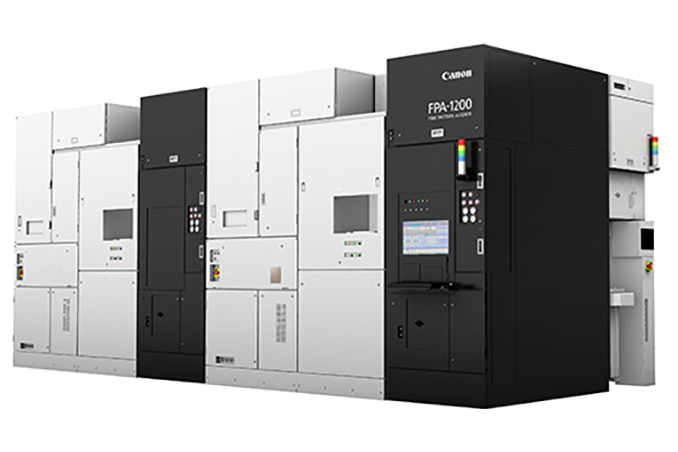
Canon made quite a splash last year when it introduced its first nanoimprint lithography (NIL) machine, which can produce chips without using traditional DUV or EUV systems. But chipmakers unfamiliar with the technique were skeptical, both of this tool and the NIL method in general. Is that changing? This week the Japanese company delivered its FPA -1200NZ2C nanoimprint lithography system to the Texas Institute for Electronics (TIE) for study, according to Nikkei.
While this might not seem like big news, it could be a major breakthrough for Canon and nanoimprint lithography. The Texas Institute for Electronics grew out of the Nanomanufacturing Systems Center of the University of Texas 'in response to growing industry interest in advanced heterogeneous integration.' The TIE is supported by a consortium of major semiconductor companies, including Intel, NXP, and Samsung. It is also supported by DARPA, which recently awarded TIE and UT with a $1.4 billion grant to build multi-chiplet 3D processors for military and civilian applications.
At TIE, Canon's FPA -1200NZ2C nanoimprint lithography system will be used for research and development by chipmakers in the consortium — which is a big deal as currently Intel, NXP, and Samsung use DUV and EUV (except NXP) lithography to make chips. Studying NIL's capabilities means these companies may eventually adopt the tech at their fabs. Canon certainly seems to be pinning a lot of hopes on these trials: It targets annual sales of 10 to 20 units over the next three to five years, according to Nikkei.
Traditional DUV and EUV photolithography systems use light to project a circuit pattern from a photomask onto a wafer covered in resist. By contrast, nanoimprint lithography directly stamps a mold — already patterned with the circuit design — onto the resist. This avoids the need for an optical system, allowing for more accurate replications of intricate designs in just one step, which could lower production costs. Lithography processes entire wafers at once, however, while NIL works serially and may be slower. NIL is currently capable of producing chips with 5nm technology and may eventually reach 2nm nodes, according to Canon.
There are many challenges NIL faces before the technology can be broadly adopted. There are still concerns about minimizing defects from dust particles during production, for example. Also, Canon will need to collaborate with other companies to create materials compatible with this new lithography method, which will be essential for widespread industry use. Finally, NIL is incompatible with flows involving DUV or EUV, making it very challenging to integrate into existing manufacturing flows; chipmakers will have to design their production technologies around NIL — which is both expensive and risky.


