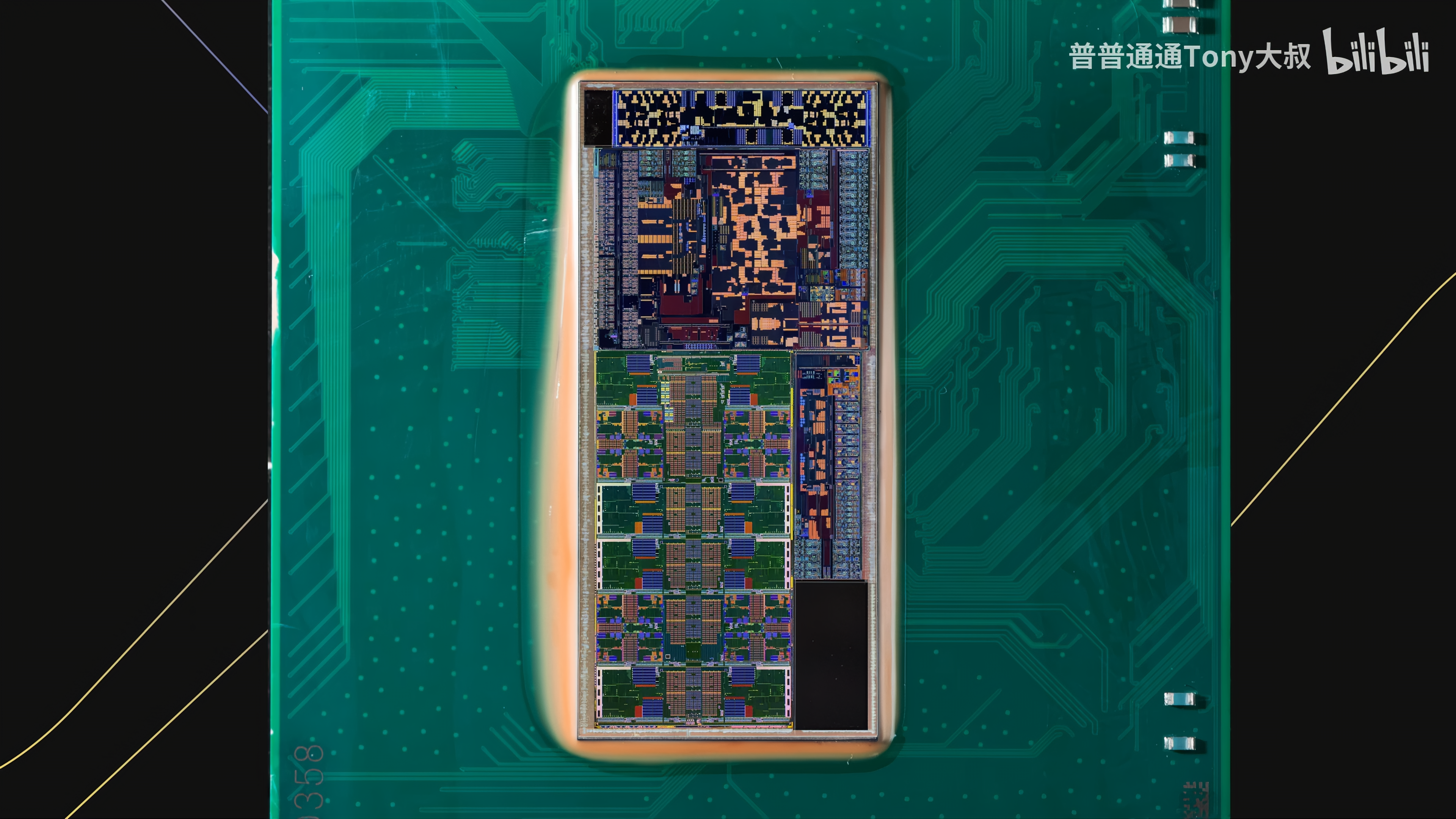
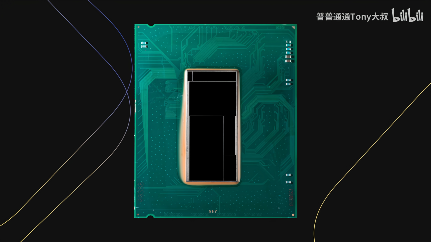
The first official die shots of Intel's Arrow Lake-based Core Ultra 9 285K have surfaced, thanks to Tony Yu at Bilibili, Asus' manager in China. The images delve into Arrow Lake's tile or chiplet architecture, structured using Intel's advanced 3D Foveros packaging technology. We also get a clearer picture of each tile's specific layout and functionality thanks to these close-ups.
Arrow Lake features a total of six tiles; the Compute Tile, the SoC Tile, the IOE Tile, the Graphics Tile, and two Filler Tiles for structural integrity. Underneath these tiles is the active interposer, which categorizes this packaging as a 3D design. Funnily enough, Intel has opted to use TSMC for every tile apart from the Base Tile - which itself is built using an outdated 22nm process node.
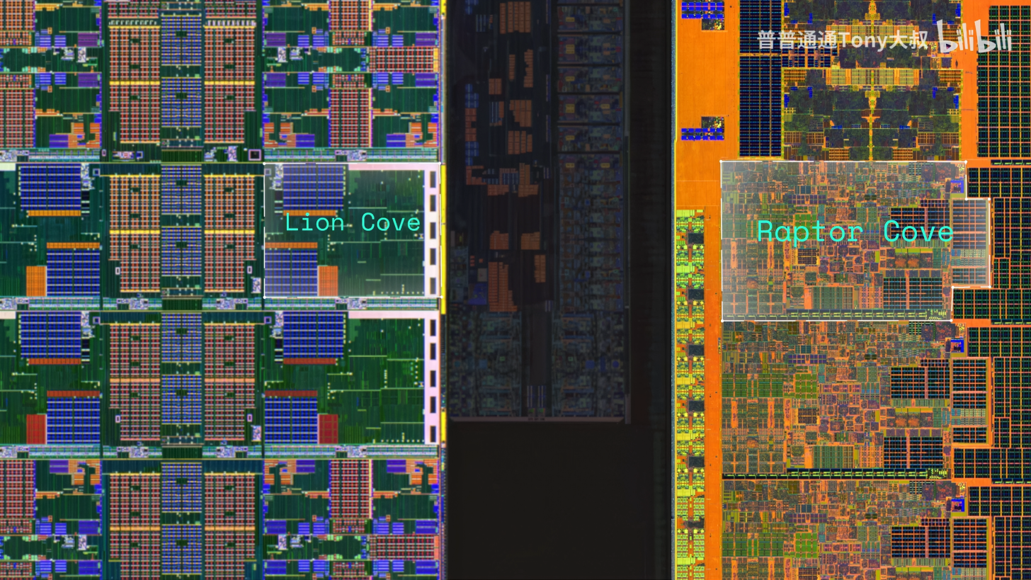
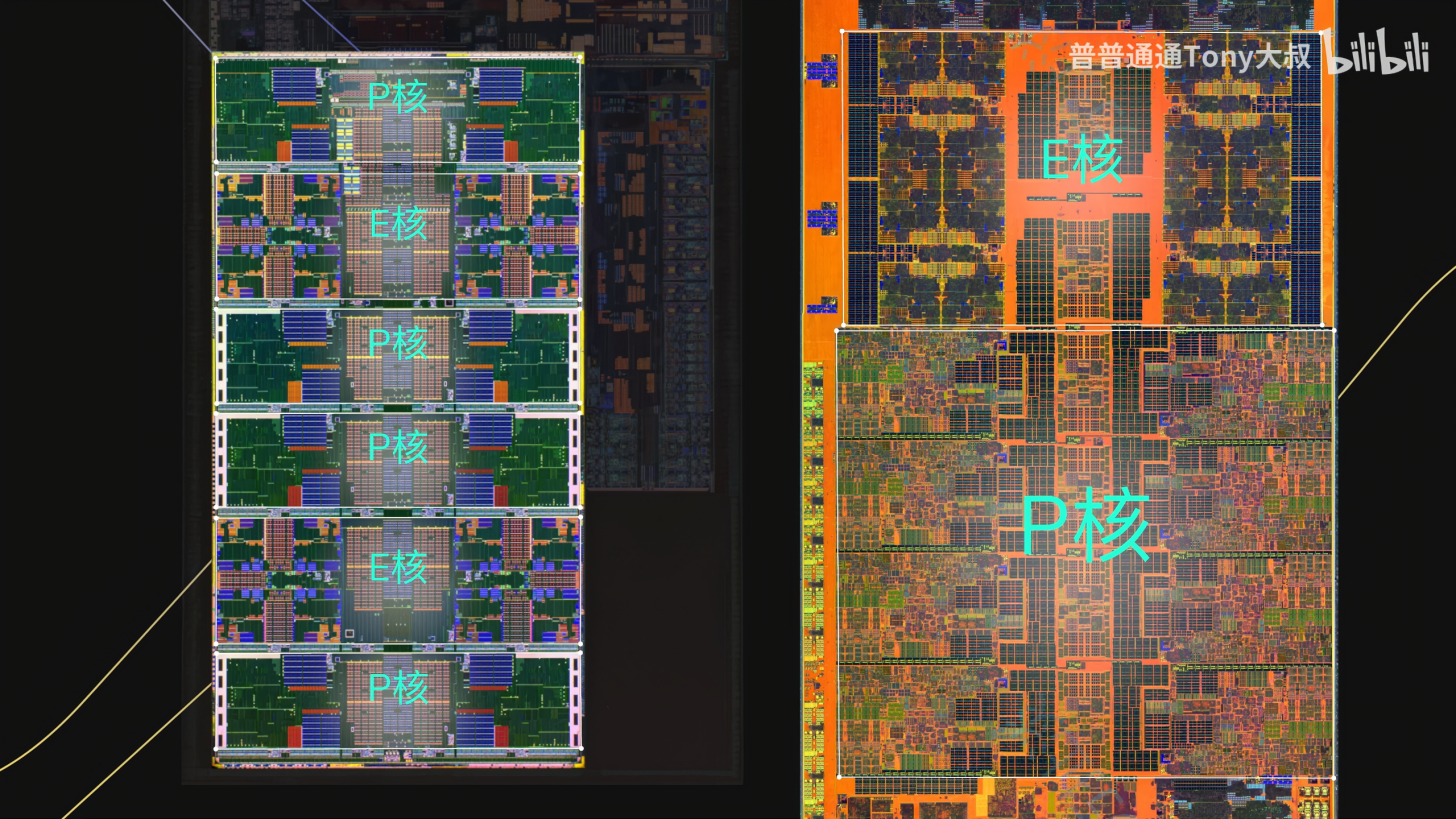
The bulk of the die space is occupied by the Compute Tile which hosts all the cores and cache. A comparison against Raptor Cove-based performance cores used in Intel's 13th Generation shows that Lion Cove is considerably smaller than its predecessor. This can be attributed to the node shrink from Intel 7 to TSMC N3B. Even the core layout is different, as Arrow Lake has the performance cores contiguous with the efficient cores, while in Raptor Lake they were placed at different areas of the die.
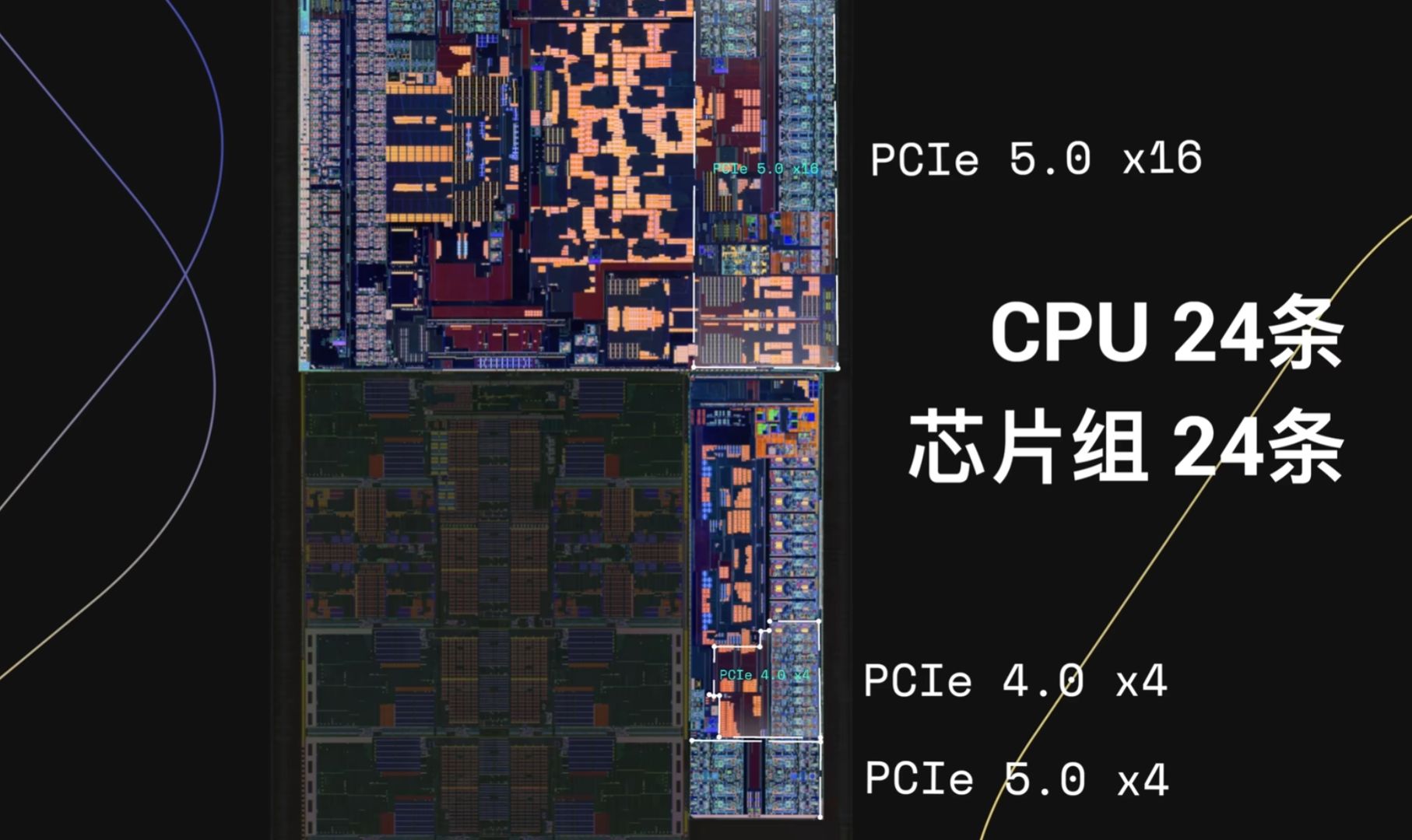
With Arrow Lake, the memory fabric and controllers have been shifted off-die to the SoC Tile - built using TSMC's N6 node. This will introduce latency penalties which, when paired with the already slow ring bus, perhaps explain Arrow Lake's poor gaming performance. The PCIe 5.0 x16 interface for the GPU is situated in the SoC Tile, though interestingly the PCIe 4.0 and 5.0 x4 interconnects for NVMe SSDs have been designated to the IOE Tile.
Furthermore, the SoC Tile also packs Arrow Lake's NPU - said to offer 13 TOPS of AI performance in tandem with the display and media complexes. Being at the center of the package, the SoC Tile will have the most Die to Die interconnects, as it has to communicate with all the chiplets. Since Intel has not explicitly detailed its core-to-uncore connection methodology, it may be safe to assume that data is still routed via the good-old ring bus.
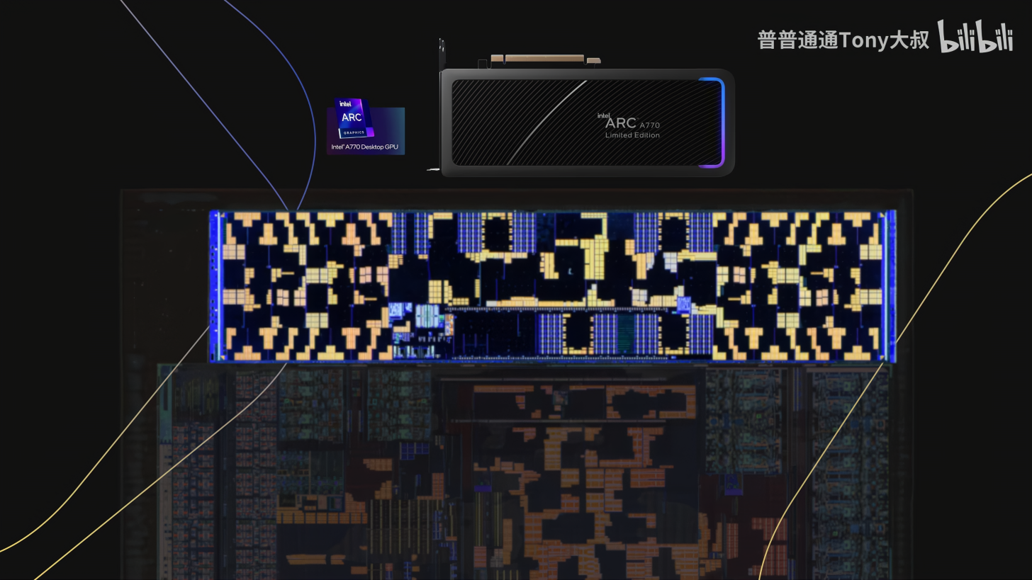
Lastly, four Xe cores based on the Alchemist architecture have been allotted to the GPU Tile - manufactured using TSMC's N5 node. This is the same Xe-LPG architecture seen in Meteor Lake and is inferior to Xe2 (Battlemage) on Lunar Lake and Xe-LPG+ (Alchemist+) expected with Arrow Lake mobile.
This disaggregated approach opens room for insane levels of modularity as Intel can swap any of these tiles according to their preferences. But, as is everything with chiplets or tiles, there is an obvious increase in latency and packaging overhead.
The Core Ultra 200S series of CPUs will hit shelves the day after tomorrow. Let's hope Arrow Lake is as good as leaks suggest. Stay tuned to Tom's Hardware for detailed reviews sharing the real-world performance of these processors.


