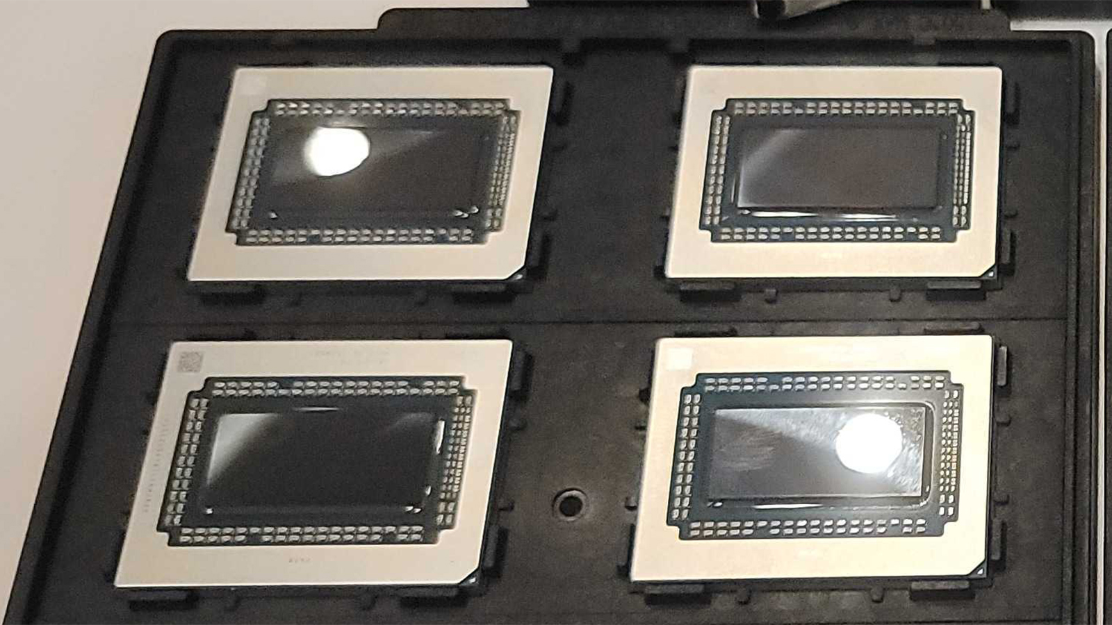
AMD's Navi 48 graphics processing unit, based on the RDNA 4 architecture that the company briefly demonstrated yesterday, is significantly smaller than its predecessors from the RDNA 3 generation. The small die size may be proof that the company does not intend to position its RDNA 4 GPUs to compete with Nvidia in the high-end market segment.
The die size of AMD's Navi 48 GPU, produced on TSMC's 4nm-class process technology, is around 390 mm², according to the calculations of blogger David Huang. The GPU is slightly larger than Nvidia's AD103, which is made on a similar process technology.
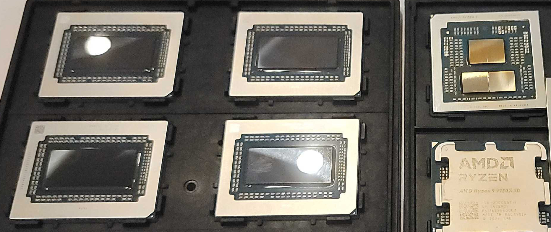
The Navi 48 graphics processor is monolithic and is not accompanied by any memory cache dies, unlike its Navi 31 and Navi 32 predecessors. This makes it impossible to make an apples-to-apples comparison between its die size and the die sizes of its predecessors. However, if we combine the sizes of Navi 3x graphics compute dies (made on N5) and memory cache dies (made on N6), we can estimate that Navi 32 uses around 346 mm² of silicon, whereas Navi 31 uses 529 mm² of silicon. These measurements roughly correspond to the positioning of the graphics processors in the performance mainstream and high-end segments, respectively. That said, it is safe to say that AMD did not aim to create an expensive GPU with its Navi 48.
TSMC's 4nm-class manufacturing technologies (e.g., N4P) belong to the same process development kit as the foundry's 5nm-class fabrication processes. These technologies provide about 1.06x higher transistor density, up to 11% higher performance (at the same power and transistor count), or up to 22% power reduction (at the same speed and transistor count). While N4P offers noticeable advantages over N5, do not expect a major performance improvement from adoption of a new node alone. Thus, any performance improvements in RDNA 4 or the Radeon RX 9070 XT over existing offerings are likely the result of architectural enhancements rather than the adoption of a new node.
In theory, AMD could adopt N4C for a higher transistor count at 390 mm² and/or up to 8.5% reduced costs. However, that would come at the cost of performance, making adoption of this node unlikely for a GPU.
When AMD first showcased the Navi 48 GPU yesterday, it was presented as the company's Hawk Point Refresh processor. However, it certainly resembled the Navi 48 GPU from AMD's press materials, not a Hawk Point CPU. We asked AMD for clarification, but the company declined to comment. As such, and when comparing to the company's other press materials, logic dictates this is in fact the first sighting of RDNA 4.


.jpg?w=600)